RF Enclosure Mini-Extended-FX: a new universal enclosure for RF circuits
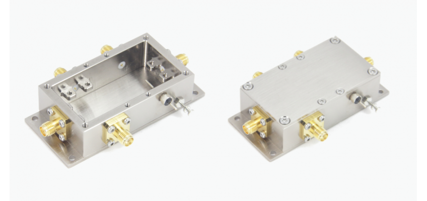
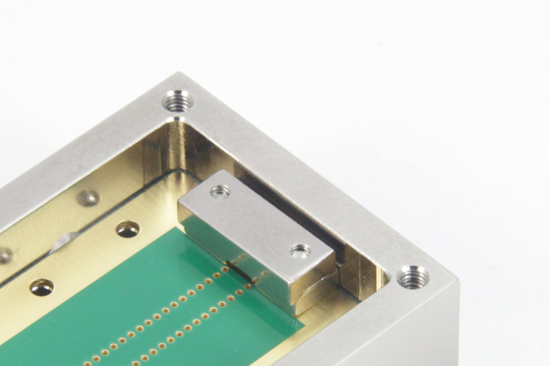
The RF Enclosure MINI-EXT-FX is a new line of RF enclosures that speed up your RF development project by creating housing, high-performance SMA ports, RF grounding, and thermal stability all in one go. Best of all, replacing the PCB with a new revision is easy, so the enclosure can be reused for your next project.
The RF MINI-EXT-FX can be conveniently used in small-series production.
The EXT designation refers to the doubled length of the PCB that fits in the enclosure, compared to the MINI version. The FX suffix refers to the combined PCB mounting and SMA port construction. This new construction makes it possible to use any PCB thickness between 0 and 1.6 mm (63 mil) while keeping the port’s VSWR to a minimum.
1. What you get
- An enclosure constructed from aluminum parts milled with high precision
- The ability to easily replace your PCBs
- An enclosure that can be configured with one to five SMA ports and SMA cover plates designed to cover unused ports
- SMA ports and PCB mounts designed for a low VSWR, assuming a GCPW transmission line–style landing pattern
- DC power terminals in the form of a turret terminal and feedthrough capacitor
- Design flexibility with regard to the PCB thickness: 0 to 1.6 mm (63 mil)
- Support for double-sided PCBs
- Excellent EM shielding
- A significant amount of thermal mass because of the milled aluminum construction
- An enclosure that is fully documented, both mechanically (i.e., drawings) and from an RF engineering viewpoint (S-parameters using reference design)
2. How you can use it
This enclosure is designed for three typical use cases.
2.1 Professional RF prototyping
This enclosure is well suited to a professional way of doing RF prototyping. No more unshielded RF PCBs lying around on the desk. By using the RF Enclosure MINI-EXT-FX, you immediately create a well-defined electrically and mechanically repeatable RF environment. You get the high degree of EM shielding that is often necessary for testing RF applications. And the enclosure gives the electronics it houses an environment with much better temperature stability.
To facilitate a rapid prototyping process, the enclosure is designed to make it very easy to replace the PCB. You can easily upgrade the PCB with a new revision or use the enclosure for a new product design altogether. Thus, by using just a few MINI-EXT-FC enclosures, engineers can always create a prototype of the new RF product they’re working on.
2.2 PCB fixture
The second use case is as a PCB fixture. In this situation, the PCB populates some devichttps://www.gquipment.com/index.php?controller=attachment&id_attachment=33e under test, and the combination of the enclosure and the PCB is used to make it accessible through the (configured) SMA ports. Typically, the DUT is an SMD component. Because the MINI-EXT-FX is equipped with a DC power port, both passive and active parts can be used.
2.3 Small-series production
Finally, the enclosure is used for small-series production by product development departments, research labs, and universities.
3. Port configurations
3.1 SMA ports
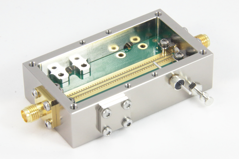
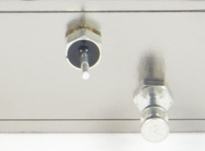
The enclosure supports up to five SMA ports. Four of them are optimized for best VSWR performance. One is optimized for the least use of PCB real estate and therefore compromises VSWR performance at higher frequencies. The first four SMA ports are arranged as shown in Illustration 1. As can be seen, the enclosure is optimized for EM waves traveling between two opposite ports. Of course, EM waves can be split and combined as the application requires. The fifth SMA port is situated in the area optimized for maximum real estate, so it isn’t combined with a PCB mounting point. This part of the PCB can be used to place components and/or route signals. This area is typically used for placing power supply components, perhaps an MCU or a communications chip to control the device from the outside using port 5. But, of course, the area can be used for whatever purpose it is needed.
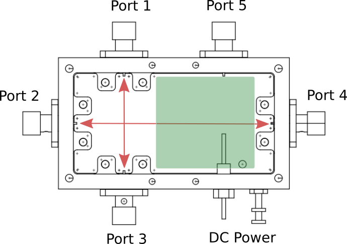
3.2 DC port
The DC port can be used to bring power to the PCB. A turret terminal is used to attach a ground potential to the aluminum body. A feedthrough capacitor is used to apply DC power.
4. PCB dimensions
The following dimensions should be used for the PCB:
- Length : 53.4 mm
- Width : 26.8 mm
- Thickness : 0 to 1.6 mm (63 mil)
Because the PCB is positioned at approximately half the height of the enclosure, both sides of the PCB can be populated.
There are reference designs to give the designer a quick start (see section 6 'Product information').
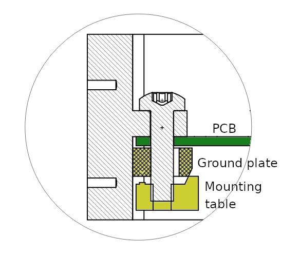
5. PCB-mounting system and SMA port construction
The MINI-EXT-FX uses a unique PCB-mounting construction that can handle a wide range of PCB thicknesses while creating a low VSWR SMA port transition to the PCB landing area and maintaining a short RF ground pad from the PCB to the enclosure. Because the PCB is positioned at about half the height of the enclosure, the ground planes of the PCB (top and bottom) are in contact only with air. Therefore, the designer has the freedom to remove parts of the ground planes to create some desired effect (for example, to minimize capacitance around component pads).
Additionally, the PCB mounting system can be easily assembled and disassembled repeatedly to reuse the enclosure for new designs.
All these effects are created by mounting pads integrated into the enclosure’s aluminum body. These pads are designed to facilitate the EM wave traveling through this construction into the PCB, thereby acting as a transmission line (GCPW). The mounting pads are complemented by a metal part that functions as an extension of the (bottom) ground plane of the PCB. This metal part is pressed into the aluminum wall of the enclosure to ensure a good RF ground connection. The pressure is created by two screws driven into a third metal part, the “table.” Illustration 2 shows the complete construction with all the parts working together.
6. Product information
You can find more information about the RF Enclosure MINI-EXT-FX in its data sheet.
To order the enclosure, you can use these links:
PCB reference designs: