De-embedding S-parameters to remove the effects of a test fixture.
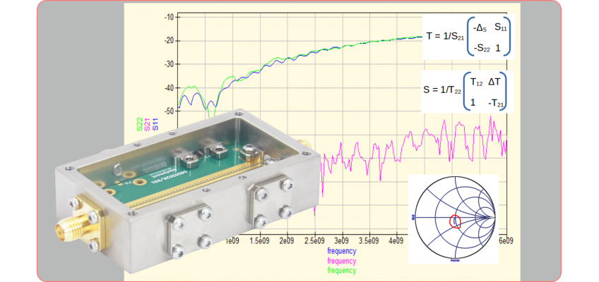
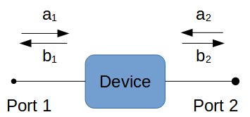
Performing S-parameter measurements on RF components can be quite challenging. The problem arises from the fact that the connections of typical RF components, for example SMD components, cannot be connected directly to a VNA because, of course, they do not have coaxial connectors. Therefore, some type of fixture is needed that houses the SMD part and connects it to coaxial connectors (Picture 1). However, this fixture with its connectors and 'wiring' will affect, often seriously, the measurement of the RF part under investigation. In this article, we outline a method using T-parameters to remove this effect from the VNA measurement.
1. Influence of the Fixture on S-parameters Measurements
The first step is to better understand how the test setup affects the measurement. We will do this by comparing an ideal situation where the fixture would have no effect whatsoever on the measurement with the more realistic case that takes the effects of the fixture into account.
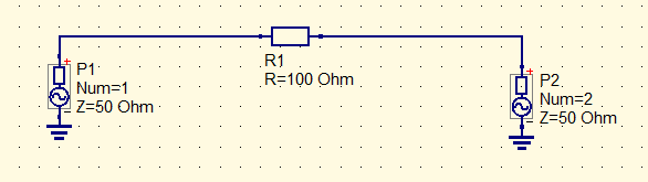
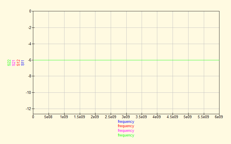
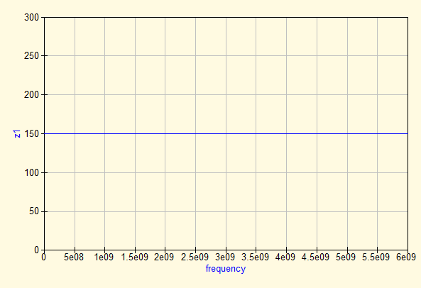
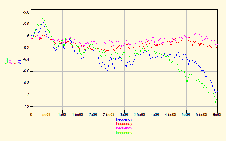
In the ideal case (figure 1) a resistor would be connected directly to the ports P1 and P2. These would then correspond with the actual measuring ports of the VNA. In this situation, there is no mismatch or any other cause that will influence the measurement of the resistor. A simple simulation of this circuit generates the S-parameter plot and impedance graph of a 100 ohm series resistor (figure 2 and 3). The four Sxy parameters happen to be all equal to -6dB. The impedance of the 100 ohm is shown as 150 ohm because it is in series with the 50 ohm reference.
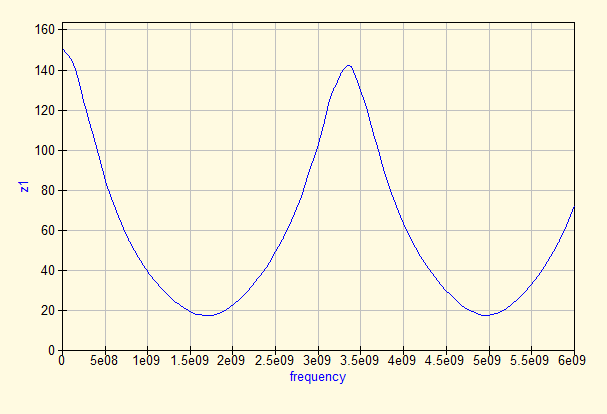
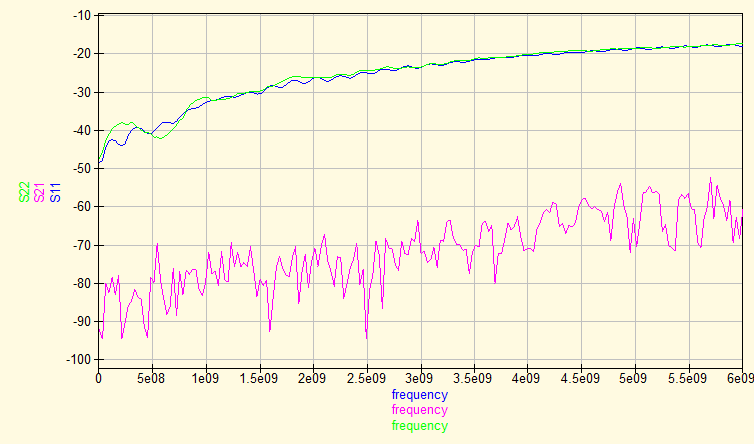
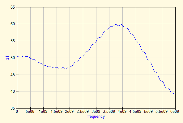
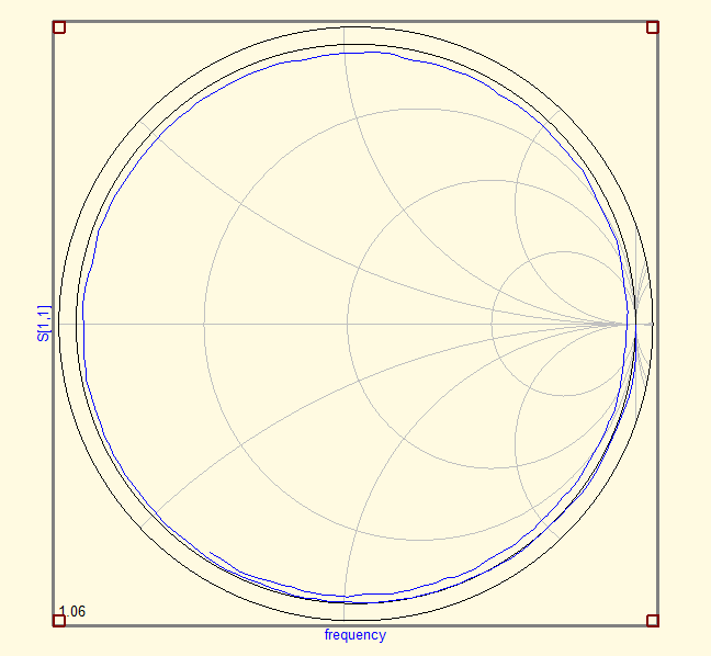
Of course, in practice we cannot ignore the influence of the fixture. It introduces reflections, phase change and attenuation of the signal. The effects of this are shown by taking a real-life measurement of the resistor using the fixture shown in Figure 1. The results are shown in Figures 4 and 5. From these graphs it is clear that there is a deviation from the ideal S parameters, although not disastrous. However, the impedance diagram is quite disturbing, with an impedance variation between 19 and 150 ohms. The latter effect is caused by the length (L) of the transmission line which will change the reflection coefficient with e-jβL, with β equal 2π/λ.
2. How to Remove the Effects of the Test Fixture?
There are several ways to remove the effect of the test fixture form a S-parameter measurement. All with their own pro's and con's. We will treat the most common ones.
2.1 Port extension
What this method does is move the reference plane of the VNA ports. In this case towards the pads of the SMD resistor. In this way, the phase error caused by the length of the fixture's microstrip and connectors is eliminated. Although this method does not compensate for errors due to reflections and attenuation, it can be very effective if this is not too much of a problem. Port extension is specified by introducing a delay (usually in picoseconds) into the VNA. This delay is then applied to all Sxy measurements and twice this delay to all Sxx (reflection) measurements. Because a reflection measurement involves both the forward and backward traveling wave.
The advantage of port extension is that almost every VNA supports it and it is very easy to use. Its main disadvantage is that it cannot compensate for other sources of error, such as attenuation and reflection.
2.2 Using T-parameters to Remove the Effects of the Test Fixture
Another approach is to remove the effects of the fixture from the measurement data. The obvious way is to measure or model the S-parameters of the fixture without the DUT and use this data to compensate for the fixture + DUT measurement data. Looking at the fixture from Figure 1, you can see that it is a symmetrical device with the DUT (the SMD resistor) in the center of the microstrip. So it makes sense to measure or model both sides to get two S-parameter matrices. One for the left side (SFixt,L) and one for the right side (SFixt,R).
If you could multiply S-parameter matrices to model a cascaded system, it would be simple to model the system as 'Smeas = SFixt,L * Sdut * SFixt,R. And Sdut would then be equal to Sdut = SFixt,L-1 * SMeas * SFixt,R-1. However, this is not correct for S parameters. But it is possible by using T parameters. With these types of parameters, matrix multiplication is similar to modeling cascading systems. So the following formula can be used to remove the effect from both sides of the fixture:
Tdut = TFixt,L-1 * TMeas * TFixt,R-1
The multiplication by TFixt,L-1, removes the effects of the left side of the fixture mathematically, because SFixt,L * SFixt,L-1 = I (unity matrix). The same line of reasoning applies for the right side of the fixture.
But how do we get those T parameters? By using a transformation to change an S-parameter matrix into a T-parameter matrix, as described in section 3.1. It is also possible to perform the transformation in the opposite direction, which is what we will need to transform the Tdut back into an S-parameter matrix Sdut.
3 Other Type of Parameter Matrices
We already talked about T-parameters, but without introduction. By the way, different parameter types exist, each with their own specific properties and use cases. S-parameters are especially useful for measuring an RF circuit because all connections are terminated at a convenient (reference) impedance Z0. The parameters represent a ratio of incident and reflected waves, giving it useful meanings such as return loss, insertion loss, gain and isolation.
Z parameters also exist. They are defined as a ratio between a voltage and a current flowing in a port. It should come as no surprise that their parameters represent impedances. Z parameters are defined under the condition that the ports are open, which is difficult to maintain at RF frequencies.
In a similar way there are Y parameters. They represent a ratio between a current and a voltage at a port and therefore represent an admittance. They are defined under the condition that the port is shorted.
Another common parameter set are the h-parameters. Here, the voltage and current ratio's are defined such that all Hxy parameters are in agreement with the physical parameters of the small signal hybrid-pi model of a (low frequency) transistor. h-Parameters are defined assuming both open and shorted ports (depending on the parameter indices). Which again is a challenge at RF frequencies.
Another common parameter set is the h-parameters. Here the voltage and current ratios are defined such that all Hxy parameters are consistent with the physical parameters of the small-signal hybrid-pi model of a (low-frequency) transistor. The h-parameter definitions use both open and shorted ports (depending on the parameter indexes). And that is again a challenge at RF frequencies.
All these parameter types can be converted into each other. There are also ABCD matrices, but we won't go into that further.
A general difference between the Z, Y, h and ABCD parameters on the one hand and the S and T parameters on the other, is that the former are all defined in terms of port voltages and currents. While the S and T parameters use incident and reflected (power) waves. The latter are also called scattering parameters.
Because scattering parameters are defined with ports terminating in an impedance of usually 50 or 75 ohms, they are much easier to measure at very high frequencies. Therefore, scattering parameters are used for RF circuits.
3.1 T-parameters to Model a Cascade of RF Modules
Now it's time to properly introduce the T parameters. They are similar to S-parameters in that they too are defined as a ratio of incident and reflected waves. But they are now defined in such a way that the waves on port 1 relate to port 2. The parameters of a T-matrix are also called transmission parameters. The use case of T-parameter matrices is that a matrix multiplication calculates the T-matrix of the cascaded circuits. So if we have module M1 and module M2 with their respective matrices TM1 and TM2, then Tcas = TM1 * TM2 is the matrix of the two cascaded modules.
The T-matrix parameters are defined as:
For your convenience, we repeat here the definition of the S-parameter matrix. Notice how the incident and reflected waves are arranged differently.
The transformation from S parameters to T parameters is defined as:
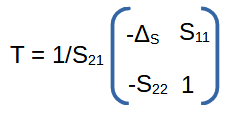
with ΔS = S11S22 – S21S12
And back from T to S-parameters as:
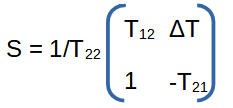
with ΔT = T11T22 – T21T12
4. De-embedding a Test Fixture with T-parameters in Five Steps
In this section we describe the complete procedure for de-embedding a test fixture. In our approach, the de-embedding is done on a local PC using a Matlab/Octave script.
We again take the same example of the test setup with the series resistance of 100 ohms. The parts used are:
- RF-ENCL-MINI-NF-01 housing is used as a test fixture
- The default brass, gold plated, SMA connector (rated for 18 GHz)
- FR4 PCB with part number 08003006/R01 (microstrip).
- 100 ohm 0402 SMD resistor, Vishay Dale Thin Film, part number FC0402E1000BTT0. This resistor is mounted exactly in the center of the microstrip.
Step 1: Model the fixture and generate S-parameter files
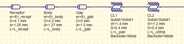
The first step is to accurately model the fixture. However, in this example we use a fairly simple model that splits each side of the fixture into three parts: the SMA connector receptacle, the part where the Teflon and its solder pin pass through the (aluminum) wall of the fixture and finally the microstrip that connects with the SMA resistor (the DUT). A more complicated model could also model the landing pad of the SMA connector. But we'll ignore that for now.
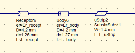
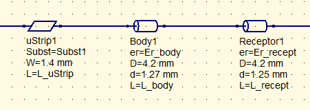
It is important to correctly model the different media in the connector and the substrate, as this has a major influence on the propagation velocity. In this example the VNA is connected to the 'Receptor' (SMA receptacle). The reference plane for all subsequent VNA measurements is also located there.
When the modeling is finished, the S-parameter files can be generated. We call them SFixt,L and SFixt,R.
When modeling is complete, the S-parameter files can be generated. We call them SFixt,L and SFixt,R.
Step 2: Measure the DUT (using the test fixture)
This is followed by measuring the S-parameters of the DUT using the test fixture. This is as straight forward as it can be. We will call this S-parameter set SMeas.
Step 3: The De-embedding Process
In this example, we used an Octave script to read the three S-parameter files SFixt,L, SFixt,R, and SMeas. If they do not contain the same frequency resolution (number of points), the lower resolution matrices are modified by inserting the missing intermediate points using interpolation.
Subsequently, all three matrices are transformed into T-matrices and a Tdut matrix is calculated using the formula Tdut = TFixt,L-1 * TMeas * TFixt,R-1. This matrix is transformed back to S parameters, so that we get Sdut. And that's the result we were looking for.
Step 5: Validate the de-embedded S-parameter matrix
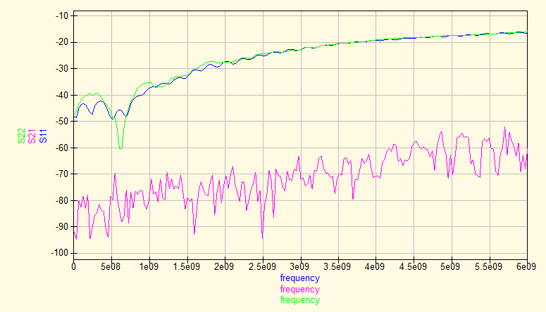
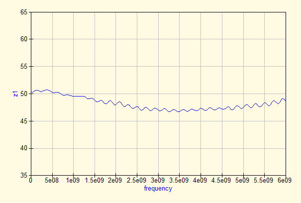
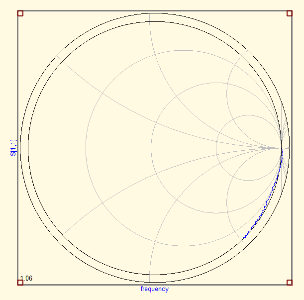
De-embedding removes the effects of the fixture. So Sdut should now contain the S parameters of a 100 ohm resistor, as described in Figures 2 and 3. We will therefore display the S parameters and the impedance Z1 for the Sdut (Figures 8 and 9), so that we can easily assess how successful the de-embedding process has been.
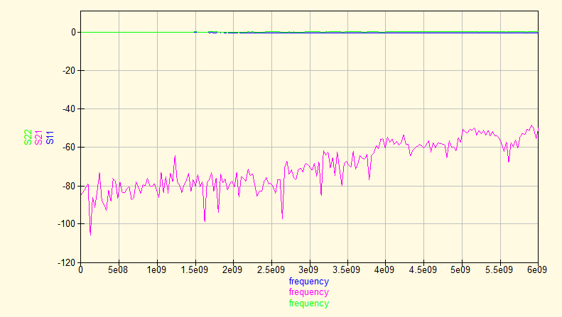
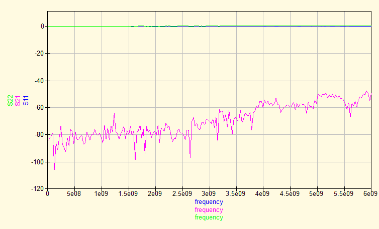
The graph of the de-embedded S-parameters shows that below 5 Ghz, the return loss is closer to the theoretical value of -6 dB. Insertion loss looks a bit suspicious as it starts to rise above -6 dB from 3 GHz onwards. Here the de-embedding process more than compensates for the actual loss in the connectors and the substrate. It appears that the model of the fixture is not accurate on this point.
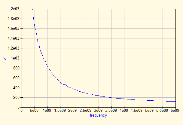
The impedance graph (figure 9) shows a huge improvement. It is clear that the phase change effect (e-jβL) of the connectors and microstrip has been virtually completely removed from the original measurement.
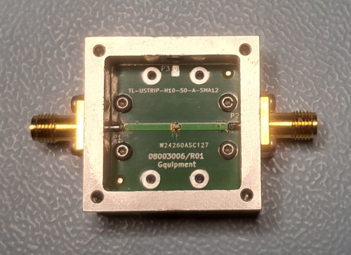
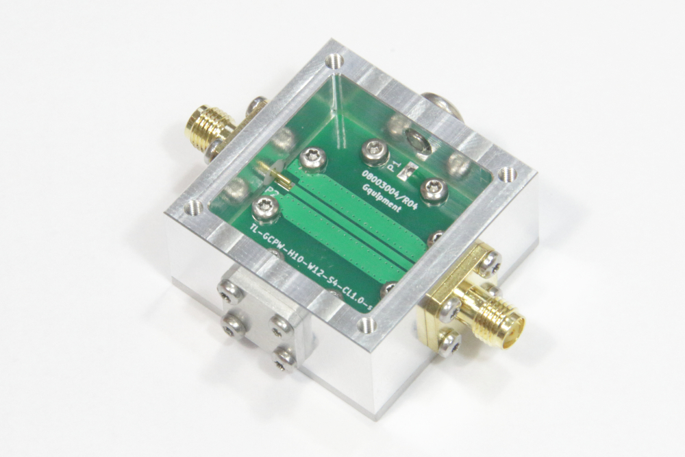
5. De-embedding a 50 ohm Termination Resistor and an Open
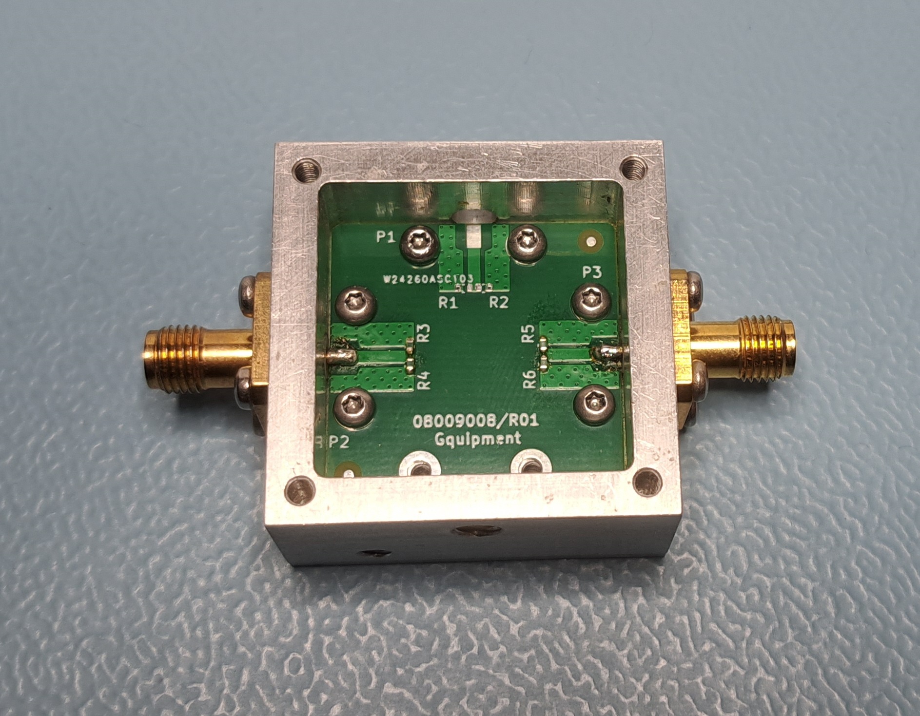
We use the same test setup again. But this time we want to measure a 50 ohm load terminating a grounded coplanar waveguide (Picture 2). This time we put a little more effort into modeling the SMA landing pad on the PCB (Figure 10). The 50 ohm load is formed by using two 100 ohm resistors, which also keeps the inductance low.
The bill of material:
- RF-ENCL-MINI-NF-01 housing as test fixture
- The selected SMA connectors of the RF-ENCL-MINI-YF-01 are of the SMA 12.4GHz type (the default SMA 6 GHz is not recommended for de-embedding purposes).
- FR4 PCB with part number 08009008/R01 (grounded coplaner waveguide).
- 2x100 ohm 0402 SMD resistor, Vishay Dale Thin Film, part number FC0402E1000BTT0. This resistor are mounted at the end of the GCPW.
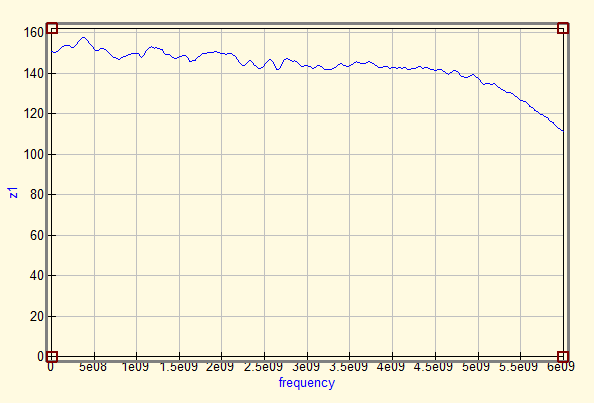
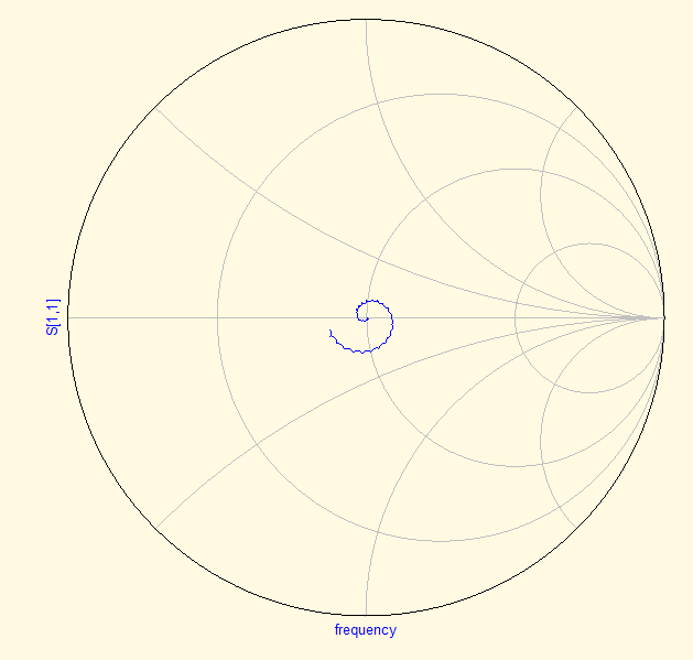
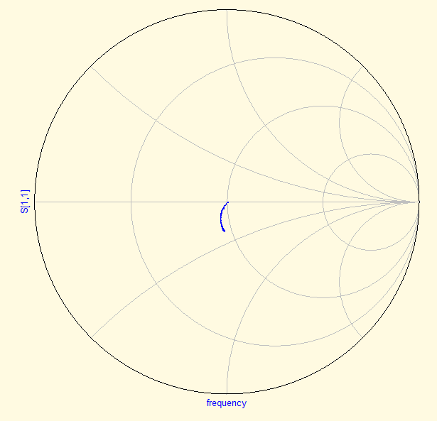
The first step is to measure the S parameters (figure 11). We also show the impedance and a Schmit chart (figures 12 and 13). The S-parameters chart shows that the return loss remains well below -18 dB, which is to be expected. The impedance plot and the Schmith chart show the known cyclic change in impedance due to the length of the transmission line (and the impedance mismatch).
We then de-embed the measurement using the steps described in section 4. In the figures below you can find the results for the de-embedded S-parameters, impedance and Schmith chart. The S-parameter plot is not very interesting. The impedance plot shows that the de-embedding process removes the effects of the transmission line. The Schmith chart shows that the load is actually a 50 ohm resistor with some parallel capacitance.
5.1 Measurement of an OPEN
We also measured an Open with the same test setup, simply by leaving out the resistors. We again show the S-parameters, impedance and Schmith chart before and after de-embedding. The return loss measurements reveal not much information, as it does not show phase information. The impedance of the raw measurement shows the characteristic impedance change over frequency of a transmission line with one end open. At DC, it start with a 'infinite' high impedance, and it flips between zero and infinity with a λ/4 interval.
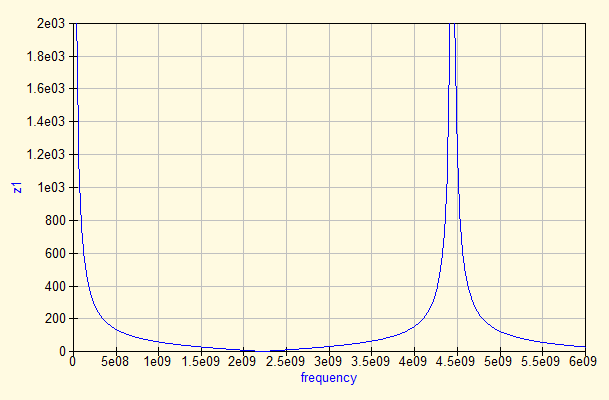
After de-embedding, the situation becomes clear most quickly by looking at the Schmith graph. It immediately reveals that the Open behaves like a capacitor, caused by the fringing fields at the end of the transmission line. Reading the chart shows that at 1 GHz the capacitance is 19 fF and increases to 23 fF at 2.8 GHz to remain constant up to 6 GHz.
6. Test fixture considerations
When looking for a test setup, there are some considerations you should take into account. The RF enclosures presented here have a few distinctive advantages. We list the most important ones:
- They are very economical solutions. An RF enclosure used as a test fixture provides good RF performance at a fraction of the cost of more specialized test fixtures.
- It is important that the return loss from the ports is not to bad. A good figure of merit is less than -20 dB over the entire frequency range.
- Probably most importantly, the repeatability of the connector port and SMA landing pad must be excellent. Otherwise, the results of the de-embedding process will contain random errors.
- The test PCB connecting the connector to the DUT must have a well designed transition from connector to transmission line to keep the return loss of the complete system as low as possible.
- In general, the length of an RF test fixture matters, but not for the model-based approach we took in this article. The test fixture used has a length of 27 mm, which fits perfectly in this case. The requirement for a longer test fixture is only relevant for de-embedding methods that rely on time-based measurements to derive the return loss as part of the solution to measure the S-parameters of the fixture.

7. Conclusions
If you want to measure an RF part, de-embedding the measurement to remove the effects of the fixture is mandatory. In this article we studied the use of T parameters to do this. The demonstration shows that making a high-quality model of the fixture is an important step. The advantage of using a model is that it can be easily adapted to changes made to the test setup.
The method presented in this article can be performed on a PC as post-processing if your VNA does not support de-embedding out-of-the-box.