Overview of RF Power Splitters, Combiners, Couplers and Hybrids
The landscape of power splitters, combiners, couplers and hybrides can be daunting at first glance. However, when we classify these devices according to their functions and take the different kinds of operating principles into account, the pictures becomes clear. To assist the RF engineer in choosing the right device for the job, we constructed an overview of these devices.
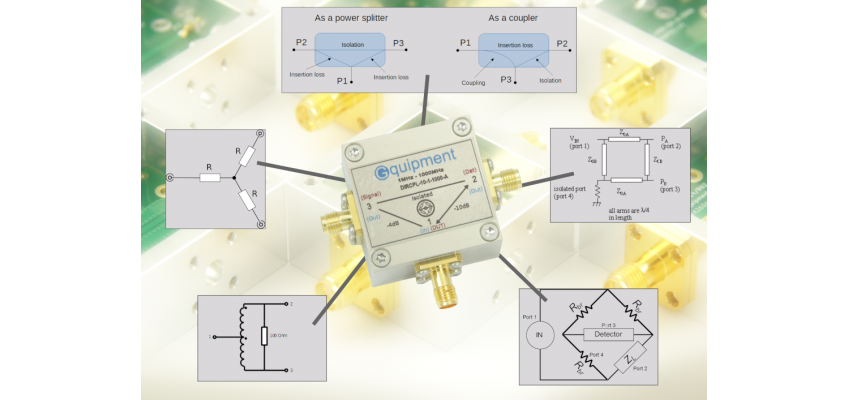
1. A Simple Model of RF Power Splitters, Combiners and Couplers
In this article, we choose to look at all devices as three-port models. Because, in most cases, that is what they will physically look like. However, some of them really are three-port devices while others are implemented as four-port devices with one port internally terminated at 50 Ohms. The latter will look from the outside like a three-port device too.
All of these devices are passive and reciprocal. Passive means that there is no power generated inside the device, in a reciprocal device there is no difference in behavior, dependent on the direction of propagation (Sxy = Syx).
These are the device models we will use in this overview:
2. Classification of RF Splitters and Couplers
The overview is organized along several dimensions. The first starts by looking at the use case. What is the main function of the device? Next we take a closer look at the general properties of the devices described by its S-parameters. However, we will not only talk about S-parameters but also about their physical, meaningful names. These are referred to as their parameters. All devices have similar parameters but their values differ a lot according to the function and the desired qualities of the device.
Next we take a look at the operating principle of the device and the technology used to implement it.
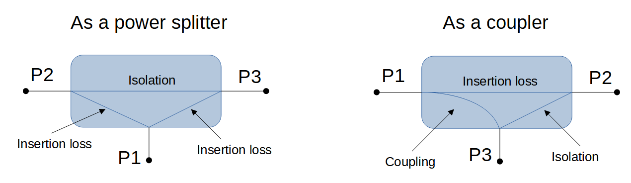
2.1 Function
The following functions are recognized.
| Function | Description |
|
|
Splits power from an input port between to output ports or (vice versa) combines two signals. It is a fairly simple operation that is commonly used in RF systems. |
|
|
Takes a sample of the signal power flow. It can be used to measure the incident power or reflected power from an RF device. For example, the output power of an amplifier or the reflection of an antenna port. |
|
|
A splitter/combiner that splits the power into two equal parts, so S21 = S31. |
|
Phase shift
|
Shifts the phase between the two output ports by 90 or 180 degrees. There are many application that use such a phase shift. Examples include modulators, balanced amplifiers, non-reflective attenuators and bias-T applications. |


Note that real life devices can often be used for more then one function. However, it is almost always optimized for one function over another.
2.2 Parameters of RF power Splitters and Couplers
Here we list all relevant device parameters. With these set of parameters, all splitters and couplers can be described. Typical values depend heavily on the type, design and specific purpose of the device. We will discuss this further in the next section.
| Parameter name | Formula | Description | Remark |
| Bandwidth (BW) | fLow - FHigh | fLow and FHigh correspond with the lower and upper -3dB points in the graph of interest. | Talking about bandwidth makes sense not only for insertion loss but also for all the other properties as well. |
|
Insertion loss |
-20Log(S21) | Insertion loss (in dB) of the forward propagating signal from P1 to P2. For the power splitter / combiner, the insertion loss from port 1 to 3 is equally important (S31). | In general, the insertion loss should be as low as possible to avoid power loss of the signal. |
| Return loss (RL) |
-20Log(Sxx) | Amount of reflected power at port X. | Reflections are a major cause of reduced signal integrity. So the return loss must therefore be as high as possible. |
| Isolation (ISOL) |
-20Log(S32) | The isolation between port 2 and 3. | The isolation of a coupler must be very high, otherwise the sampled (coupled) signal will have an large error. |
| Phase shift | arg(S21) - arg(S31) | Difference in phase between the output ports 2 and 3. | |
| Balance |
S21/S31 |
The difference in magnitude and phase between the two output ports 2 and 3. | Power splitters and hybrids divide the RF power in equal parts, so ideally |S21/S31|equals 0 dB. |
| Quadrature | arg(S21) - arg(S31) = 90 | Difference in phase between the output ports 2 and 3 is 90 degrees. | |
| Coupling (CPL) |
20Log(S31) | Amount of 'sampled' power from port1 to port3 | This terminology is exclusively used for a coupler. |
| Directivity (D) |
ISOL - CPL - IL (dB) |
The directivity is a measure for the accuracy of the power sample function of a coupler. |
A directivity of 0 dB would mean that the power sample on port 3 would have infinite error. A minimum directivity of 20 dB is often cited as an adequate value. |
Note that both quadrature and hybrid are not really properties of a device, but a constraint put on some property values as already seen in table 2. If both output signals differ 90 degrees in phase, its called a quadrature device. A quadrature hybrid is a coupler that will split input power into two output signals of the same power while creating a 90 degree phase change.
Please note that the insertion loss in a device that splits the power into two halves, will be at least 3 dB, due to the splitting of the power by a factor of 2.
2.2.1 General Remarks on Splitter and Coupler Parameters
Now that we've defined what the parameters are, it's time to take a closer look at them. The discussion is about couplers and splitters in general. In chapters 3 and 4 we will focus on specific solutions for splitters and couplers.
Bandwidth
Bandwidth requirements vary widely between applications. Ideally, the bandwidth runs from DC to daylight. Of course, this cannot be achieved with real devices and fortunately most applications do not require this.
When looking at DC behavior, it is worth understanding that some applications are better off to see no DC component at all. In this situation, a device that blocks DC is actually an advantage. An example is a sensor application where a DC component would introduce a measurement error.
On the other hand, a set of couplers is sometimes used to create a bias-T, which by definition must pass DC.
Most applications require limited bandwidth, with the narrowest range being an octave or even smaller. Such devices can be designed with low insertion loss. The same applies to devices that need to cover multiple octaves. These octaves can be placed almost anywhere on the spectrum.
Spanning several decades is also possible, but designs based on magnetics and/or resistors will be required to create the large operating range. Usually the insertion loss will suffer from these solutions.
Insertion loss
For hybrid power splitters and combiners, the insertion loss values are either 3 dB for a lossless design (caused by splitting the power into two equal parts) and 6 dB for devices that dissipate power (by using resistors). These are the theoretical values, which can be approached reasonably well.
Insertion loss in a coupler is a trade-off between the coupling and the insertion loss. In general, the insertion loss is lower and the coupling is higher than 6 dB. This way the device doesn't attenuate the power flow it samples too much. Higher coupling is not a major problem for most applications, so this trade-off makes sense.
Return loss
Generally higher is better here (lower reflections). 20 dB can be considered a very good value. The higher the return loss, the less signal amplitude variation will be created by interfering waves due to reflections generated in the port of interest.
Another consideration that is not mentioned as often is that the port of a coupler used to measure incident or reflected power must be very closely matched. So this port should ideally have a very good match (RL > 25 dB) to minimize this source of measurement error.
Isolation
Of course, the higher the better. However, the required minimum isolation varies a lot depending on the application.
For the application of combining two signal together, the goal is to decouple the signal sources so that they will not influence each other. An isolation of 20 dB or better will do this job quite sufficiently.
But if we want to make a return loss measurement with a coupler, the situation quickly becomes much more demanding. If we want to measure a D.U.T. with a return loss of -20dB with an accuracy of 3 dB using a 6dB (hybrid) coupler then that device would need an isolation of 47 dB or better! This example shows that to measure reflected power, a coupler must have very high isolation to keep the measurement errors sufficiently low.
Phase shift
Shifting phase is used for a variety of applications. For example, to cancel out unwanted reflections or to change the phase of an LO signal feeding a mixer. Ideally, the phase shift is frequency independent. In practice, however, this is a challenge. The difficulty arises because the phase shift must be created by using a transmission line or capacitors and inductors. And all these elements exhibit frequency-dependent behavior.
In practice, you can expect devices with a constant phase shift over half an octave to several octaves at best.
Quadrature
The adjective 'quadrature' indicates a 90 degree phase shift between the output ports. Shifting the phase of a signal, for example a local oscillator signal, is often used in RF designs.
Coupling
The higher the Coupling, the less power is extracted from the signal, resulting in lower insertion loss. Ideally, a coupler has an insertion loss of 0 dB and therefore a high Coupling. The exception to this is the hybrid, a device that splits the power into equal parts so Coupling and insertion loss are equal (it behaves like a power splitter).
Practical RF couplers are available in a wide range of Coupling factors, from 3 to 20 dB. The Coupling is often used as the primary value to describe the operation of the device. The second is undoubtedly its Directtivity.
Directivity
This is an important figure of merit for a coupler. Its indicates the measurement error you can expect in the power sample function of the coupler. Higher Directivity corresponds to lower error. To get a feel for the numbers involved: if you want to measure a D.U.T. witch has an expected return loss of 20dB with a maximum measurement error of 3 dB, you need a Directivity of at least 35 dB. A coupler with a Directivity of 35 dB is considered an excellent device.
Hybrid
A hybrid divides the power into equal parts between the ports. 3dB and 6 dB are quite common values. In power amplifier applications, a 6 dB insertion loss is often considered unacceptable, so you're likely to find the 3 dB version there. In R&D environments or on the test bench, power is of less concern, so the 6 dB variant is often found there due to their larger bandwidth.
3 Technology
In this section we look at the technology used to implement these RF devices and how this influences its parameters.
| Technology | Properties |
|
Resistors only
|
Usable from DC up to approx. 20 GHz, if special care is taken in resistor selection and placement, substrate selection and layout.
|
|
Lumped RLC components
|
Usable from DC to several GHz. The main limiting factors are the parasitic capacitance and (lead) inductance of the components. Inductors in particular begin to deviate from their ideal behavior at higher frequencies due to parasitic capacitance between the windings. Likewise, capacitors will suffer from serious parasitic induction if operating frequencies become high enough. To reach the GHz range, the components must be small, which is why the use of SMD components is common. The layout also has a significant influence on the achievable bandwidth. |
|
Distributed elements
|
When frequencies are too high to use lumped elements, distributed elements come to the rescue. Distributed elements are capacitors and inductors that are made using the copper layer of a PCB. Often in combination with transmission lines to transform the impedance of an element. This technique can be used from a few GHz. There is no main reason why it cannot be used at lower frequencies, other than that the size of the structures becomes too large to be practical. The upper frequency is limited only by the limitations of the substrate and copper layer and can easily extend to several tens of GHz. |
|
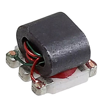
Magnetics
|
An important technology is the use of transformers that use a ferrite to increase inductance. They can be made to operate from 100 KHz to 3 GHz, all in a relatively small form factor. There is also a surprisingly large repertoire of RF designs that use transformers in one form or another. The limitations of this technology arise from the capacitance of the windings and the changing properties of the ferrite at higher frequencies, where it loses its permeability, resulting in a loss of magnetic induction in the transformer. |
|
Transmission lines
|
Usable from DC up to 10s of GHz. Although transmission lines operate down to DC, they aren't usable at these low frequencies because they would be impractically long (a quarter wave length at 1MHz is still 47.4 meter using an Er of 2.5). Therefore, transmission lines are used starting at the GHz range only. |
4. RF Power Splitter, Combiner and Coupler Designs
In this section we will summarize common designs that are used in splitters, combiners and couplers. We will point out how they impact the device parameters. So you'll get a feeling of what design will match well with a specific function.
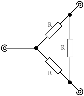
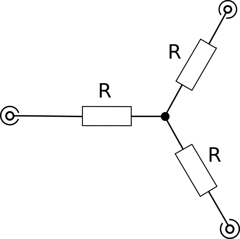
4.1 D/Y-Resistive Network
This network is used as a power splitter / combiner. The D configuration (figure 2) uses 50 ohm resistors, the circuit in figure 3 (Y configuration) consists of 50/3=16.67 ohm resistors.
Insertion loss and isolation between all ports is 6 dB. This is not a lossless splitter as half of the power (3 dB) is dissipated in the device. Hence the insertion loss of 6 dB (3dB due to loss and 3 dB caused by the power being split in two equal parts). This is a true broadband design as there are no frequency-dependent components used.
This type of power splitter is used when a signal needs to be duplicated in an RF system. You cannot simply split an RF signal due to the characteristic impedance of the transmission lines involved. For example, if you split a 50 ohm transmission line into two branches, the impedance at the intersection where the split occurs will be 25 ohms (two parallel lines). The three-resistor current splitter solves this problem because the ports all match the characteristic impedance. Likewise, this splitter is used to combine two RF signals into one. The SPLT-3R1-0-6000-B is an example of this type of splitter.
4.2 Divider Network Using Two Resistors
Although the device might look rather similar to the D/Y splitter configuration, they both are actually quite different. First, the isolation in the two resistor network between ports 2 and 3 is 12 dB instead of 6dB.
But the biggest difference comes from the fact that the impedance at port 2 and 3 are not matched to 50 ohm. This becomes clear immediately when you look at the S-matrix of the circuit as S22 and S33 are equal to 0.25 instead of (the probably expected) 0.
Insertion loss (S21 and S31) are both 6 dB. Internal power dissipation is 3 dB. Its a true broadband design because there are no frequency-dependent components used.
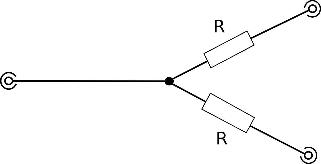
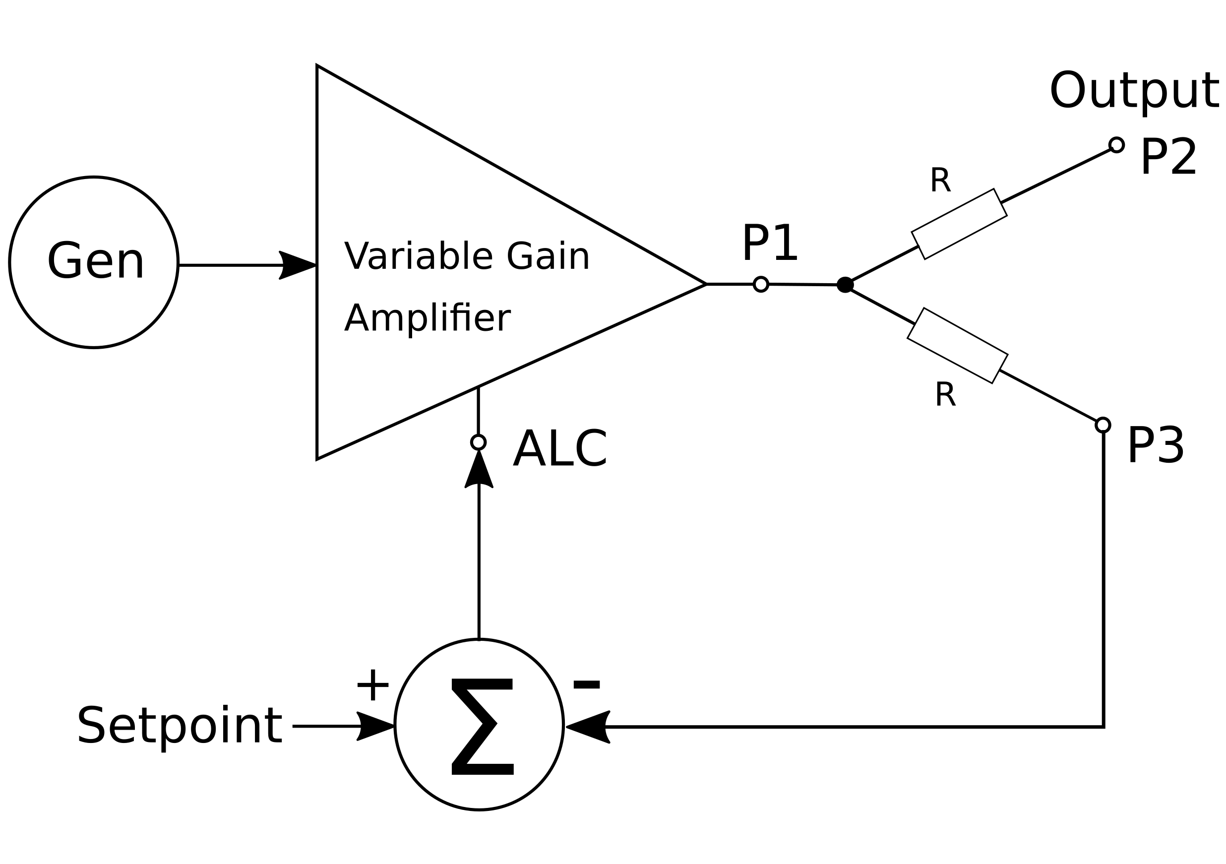
At first glance this circuit does not seem very interesting, but it has a remarkable property: the power emitted on ports 2 and 3 is always the same, even if the ports are not equally matched.
This makes this circuit the ideal candidate for measuring the power leaving port 2 by measuring the power on port 3.
A second feature of this splitter is that, when used in a negative feedback loop, the output port match will be almost perfect. This is possible because reflections at the load of port 2, which are reflected at port 2, are also emitted at port 3 (and vice versa). And because port 3 is part of the negative feedback circuit, the input power to the splitter will be reduced by the same amount. That exactly compensates for the amount of reflected power on port 2. So when we look at port 2, we see an almost perfect, effective match.
The degree of perfection that can be achieved depends on the gain of the feedback loop and on the degree of equality of the splitter's S-parameters: S21 = S31, and S22 = S33 = S32 = S23. An example of a two resistor splitter is the SPLT-2R1-0-6000-B-NF.
4.3 Wilkinson Splitter
The Wilkinson splitter splits power in equal parts. The circuit is lossless, so this is a 3 dB hybrid. This design also provides high isolation between port 2 and 3. There is no phase shift between the output ports, due to its symmetrical design. So, when splitting power, there will not flow any power through the resistor, as there is no potential difference.
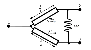
The isolation between ports 2 and 3 exists because the splitter creates a 180 degree phase shift for any signal going from port 2 to 3 (or vice versa) as it must travel through the two λ/4 transmission line segments. But that signal will also travel through the resistor, where it reaches the opposite port without any phase change. And there the two signals cancel each other out. For this to work, both signals must have the same magnitude, so the impedances of both paths must be the same. If the port impedance is Z0, the other two paths must present 2*Z0 because they are operating in parallel. The transmission line segments therefore also act as impedance transformers. Its character impedance must be Z0√2 to create the impedance doubling.
The bandwidth of the transmission line-based design is approximately one octave. However, it can be improved by cascading multiple sections. Other features that make this splitter design popular are its low cost and simple construction.
Wilkinson splitters can also use a transformer to implement the power splitting and impedance transformation. The bandwidth of the transformer-based design (bottom image) is determined by the transformer used. Normally it can span one or more decades, but the upper frequency is limited by the ferrite used and the parasitic capacitance of the transformer coil.
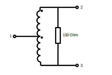
A problem of the transformer based circuit is that its input impedance is Z0/2. This is caused by the transformer which transforms impedance by a factor of 4. For this reason, there must be a circuit that transforms this 25 ohm impedance to the proper 50 ohm. Usually, this is done with a transformer too.
One problem with the transformer-based circuit is that the input impedance is Z0/2. This is caused by the transformer converting the impedance by a factor of 4. For this reason, there must be a circuit that converts this 25 ohm impedance back to the correct 50 ohms. A transformer is usually also used for this. The SPLT-MT1-1-500-A-NF is a Magic Tee that uses this kind of magnetics based solutions.
4.4 Coupled Transmission Lines
A coupler can be constructed from two coupled transmission lines. For example, by running two traces close to each other. This is a lossless circuit, so in theory, no power is wasted. This device can be used as a coupler due to the high isolation between ports 1 and 4. Port four is often terminated 'internally'. A fraction of the input power is present on port 3 (S31, or CPL). The input power is divided between P2 (through) and P2 (Coupled) in the ratio √(1-CPL2) / CPL.
To qualify a coupler as such, it needs a considerable degree of directivity (D). For this design, directivity is defined by the fraction of coupling and isolation, or D = S31 / S41. The directivity indicates the measurement error in the power measured at the CPL port (#3). This error is caused by the incident power from port 1 being reflected at port 2. Because the device is symmetrical, we can look at this reflected power as if it were coming from the through terminal. And from this view, port 3 becomes the isolated port. The reflection therefore cannot reach port 3 and therefore cannot interfere with the coupled power.
The analysis of coupled transmission lines is done by looking at the even and odd impedances (ZE0 and ZO0 respectively) of the transmission lines. It can be shown that in order to match the ports to Z0, ZE0 * ZO0 = Z02 must be satisfied and the physical structure must be symmetric (in both directions). To do this, one must modify the physical parameters of the lines, such as the geometry and substrate parameters. There is no simple mathematical solution for this, which is why in practice an RF simulator package is used to design these types of couplers.
The coupling is maximized for the design frequency when the length of the two transmission lines is λ/4. This also shows that the coupler is frequency dependent, making it a fairly narrow band device (one to two octaves at best). However, bandwidth can be improved by using multiple coupling sections in one design.
This coupler has another interesting feature, namely the phase shift between ports 2 and 3, which is always 90 degrees. What is remarkable about this phase difference is that it is frequency independent. So this is a real quadrature device.
This type of coupling is widely used in microwave PCB design because it is very cheap to implement. The coupling is usually quite high (= small power sample) to avoid unrealistically small gaps between the two coupled lines.
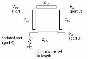
4.5 Branchline
In a branchline coupler, four transmission lines are configured as shown in figure 9. The transmission lines have a length of λ/4, ZA=Z0/√2 and ZB=Z0.
Power is split in equal parts (hybrid). The operating principle is lossless (there is no power dissipated), so insertion loss for S21 and S31 are both 3 dB due to the power split. The phase shift of port 2 is -90 and for port 3 equals -180 degrees.
That this device also acts as a directional coupler is explained along the same reasoning used in section 5.4 (coupled transmission lines), so we will not repeat that here.
The branchline coupler is analyzed using odd and even mode analyses. It can be shown that all the four ports are matched to Z0.
This is a narrow band device. However, performance can be improved by adding extra sections. Implementation cost is low and at sufficiently high frequencies the footprint is not too large.
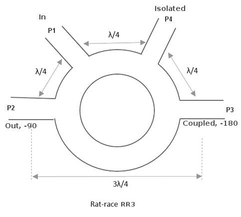
4.6 Rat-race
A rat-race coupling is made of a transmission line in the shape of a ring. It has a circumference of 1.5λ and the ports are spaced λ/4 apart. The characteristic impedance of the line segment is √2*Z0. It is a lossless design and the power is divided into equal parts. The insertion loss for S21 and S31 is therefore both 3 dB. Like all transmission line-based designs, the circuit is designed around a target wavelength λ. As a result, the bandwidth is quite narrow. All 4 ports of the rate-race coupler are matched to Z0 (at the design frequency). Usually, the isolated port is terminated internally.
It is easy to reason about the Sxy-parameters of the rat-race by looking at the two possible paths a wave can take from port X to port Y. For example, using the configuration shown in Figure 7a, a wave traveling from port 1 to port 2 can do so clockwise and counterclockwise. Clockwise it travels 360+90 degrees, counterclockwise the distance is 90 degrees. So both signals add in phase and S21 is equal to -j/√2. The √2 accounts for the power split. Similarly, a wave from port 1 to port 4 travels 360 degrees and 180 degrees respectively, so they cancel each other. S41 is therefore equal to 0.
A rat-race coupler is a versatile device because it can be used in three different ways:
a. As a hybride
The power is split (-3 dB) and there is no phase difference between the two output ports (Figure 10a). It is a good option for a power divider because of the good isolation between the output ports, the relatively small footprint and the ability to handle higher powers.
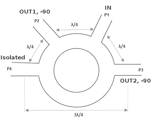
b. As a hybride with 180 degrees phase shift
The power is split (-3 dB) and there is a 180 degree phase difference between the two output ports (Figure 10b).
The 180 degree phase difference makes this configuration a popular choice for transforming a signal from balanced to unbalanced. In this application the two outputs (P2, P3) are used as balanced inputs. The input port (P1) of the rat race coupler now acts as the unbalanced output port. An application example is the conversion of a balanced RF amplifier output to an unbalanced version to feed an antenna.
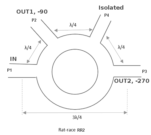
c. As a coupler
P1 is the input port and P2 is the output port ('through') when used as a coupler. Note the reassignment of port numbers to remain consistent with our model in Figure 1.
A fraction of the power reflected by the DUT (not visible in Figure 10c) on port 2 is present on P3 (coupled). P3 is isolated from input P1, giving this configuration its directivity (D). This way, a rat-race coupler can be used to measure the return loss of a load.
4.7 Resistive Bridge
A coupler can also be realized by using a resistor bridge. This allows the reflection of an unknown load (ZL) on port 2 to be measured (figure 11). Or the output power of a source is measured, where P1 and P2 switch functions. For the remainder of the discussion, we will keep the reflection measurement in mind.
Note that also port 1 and 3 can switch function. Port 1 or 3 can therefore be provided with a signal and the measurement is then carried out on the other port.
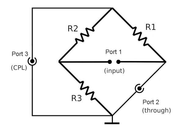
When all resistors are equal to Z0 and assuming all ports are properly terminated, it is easy to see that the bridge is balanced. In this case, port 1 and port 3 are isolated, because a signal from port 3 will not introduce a voltage difference across port 1 and vice versa.
It is possible to change the values of R1 and R3 without disturbing the balance, as long as R1*R3=R2*Z0 is satisfied. With R2 equal to Z0 (reference impedance) we get:
R1*R3=Z02
This means that R1 and R3 can be changed according to:
R1 = Z0*k and R3=Z0/k, where k is a constant.
This is useful because R1 and R3 define the insertion loss (IL, S12) and coupling (CPL, S32), respectively:
IL = 20Log[Z0 / (Z0+R1)] and CPL = 20Log[Z0 / (Z0+R3)]
When k=1 is used, IL and CPL are 6dB, making it a hybrid coupler. But usually, a coupler must have lower insertion loss, to avoid power loss in the signal path of which it is a part. So, K>1 is common for these bridged based couplers. However, too large a value of k will lead to resistance values that will place excessive demands on minimizing parasitic capacitance and inductance in the construction of the coupler.
For completeness, we also mention that it is possible to show that a resistor bridge can be used to measure the reflection caused by a load ZL by applying Kirchoff's circuit laws. For this approach, it is useful to define port 3 as the source and port 1 as the coupled port. From this analysis it follows that the voltage over port 3 is proportional to (ZL-Z0) / (ZL+Z0). We recognize this as the reflection coefficient Γ (Gama).
This coupler can also be used an RF power splitter, with high isolation between its output ports (figure 12).

The use of resistors makes this a true broadband circuit that can span multiple decades.
Note that port 3 is balanced, as it has no reference to ground. Therefore, in real couplers, a balun is added to transfer it to an unbalanced type. This balun is not shown in figures 11 and 12.
In practice, the lower frequency range is mainly limited by the balun used to connect the bridge to the coupled port 3. The higher frequency limit usually comes from the parasitic inductance around R3.
The isolation can be very high and is also maintained over the entire operating range. This makes the resistor bridge coupler the ideal choice for broadband couplers that also require excellent directivity.
This concludes the overview of splitters, combiners, couplers, hybrids and quadrature devices.