Landing Pad Design for an SMA Connector Using an RF Enclosure MINI
A common problem with almost any RF design is how to make a good connection between the coaxial connector and a signal trace on the circuit board. Several impedance transitions and/or changes in direction of the EM field play a role here, which cause unwanted reflections that disrupt and distort the signal. In general, this phenomenon already starts to play a role at frequencies above 1 GHz. The amount of signal reflection is expressed as Voltage Standing Wave Ratio (VSWR) or return loss (RL). In this article we will use return loss because it is a more suitable number to express very low signal reflection values.
Good return loss is crucial in many application areas. For example, with measuring equipment such as a VNA or a power meter, a poor return loss from the measuring port will have a negative effect on the measuring accuracy. And staying in the measurement domain, when using a PCB fixture with coaxial ports to measure an SMD component, a port with poor return loss will obviously also negatively impact accuracy. Another example is the reduced performance of an antenna system caused by a bad return loss in the feed line. Finally, when large amounts of power are involved, the reflected power can be sufficient to destroy components that are 'upstream'. Please note that poor return loss (high VSWR) also introduces higher voltages which can also cause damage.
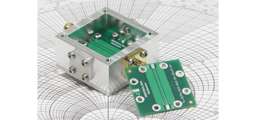
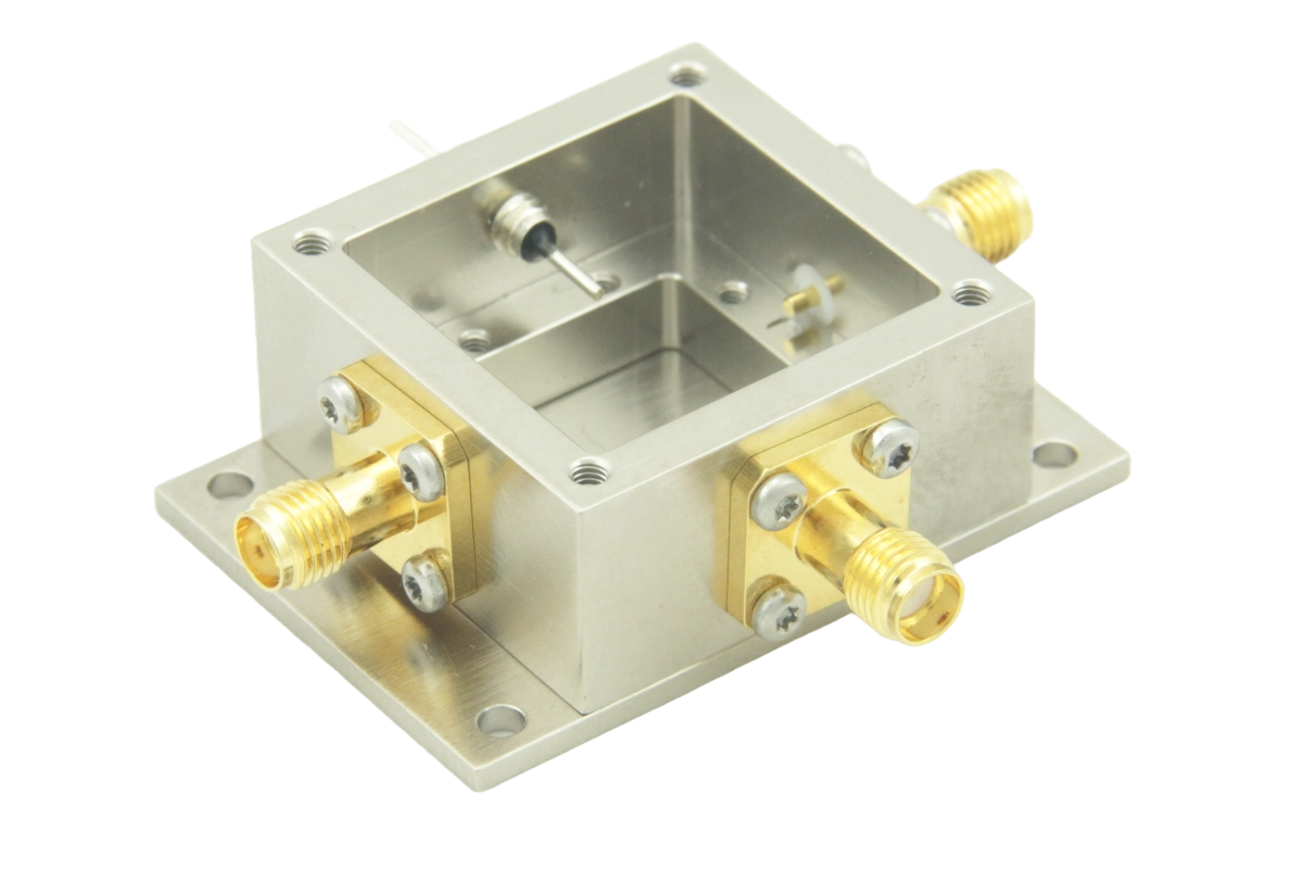
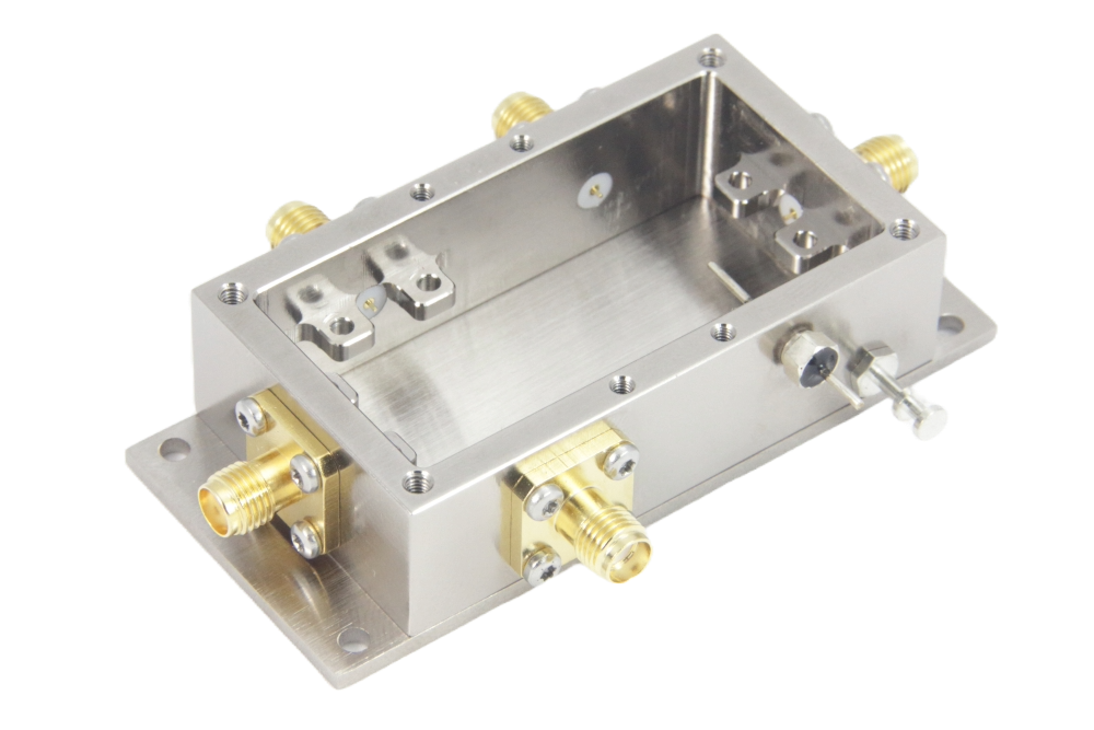
In this post we'll show you how to design a transition from a coaxial connector to a PCB landing pad with low return loss. We do this for the panel-mounted SMA connectors used in the RF-ENCLOSURE-MINI series.
1. SMA Connector to Landing Pad Transitions
When trying to understand what an RF signal encounters as it travels from an SMA coaxial cable to a signal trace on the circuit board, it helps to divide the signal path into individual segments. A transition takes place at the edges of these segments (arrows in the figures below). Figure 1 shows an example of a panel-mounted SMA connector. At each transition, the RF signal enters a new area that is modeled as a type of transmission line.
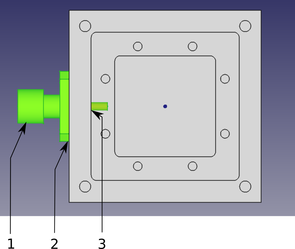
The first transition ('1') begins where the SMA coaxial cable connector mates with the panel-mounted SMA connector. This is also a handy place to position our reference plane (as you would when using a VNA). With this transition we enter the SMA receptacle, which is modeled as a coaxial transmission line. The next section is the body of the SMA connector ('1'-'2'). In many cases this segment can be modeled as part of the receptacle by increasing its length accordingly. The third segment is where the Teflon extension goes through the aluminum wall of the housing ('2'-'3'). This is modeled as a coaxial transmission line with a copper inner wire, a Teflon dielectric and an aluminum outer screen. The dimensions are determined by the SMA connector and the diameter of the hole in the wall of the enclosure.
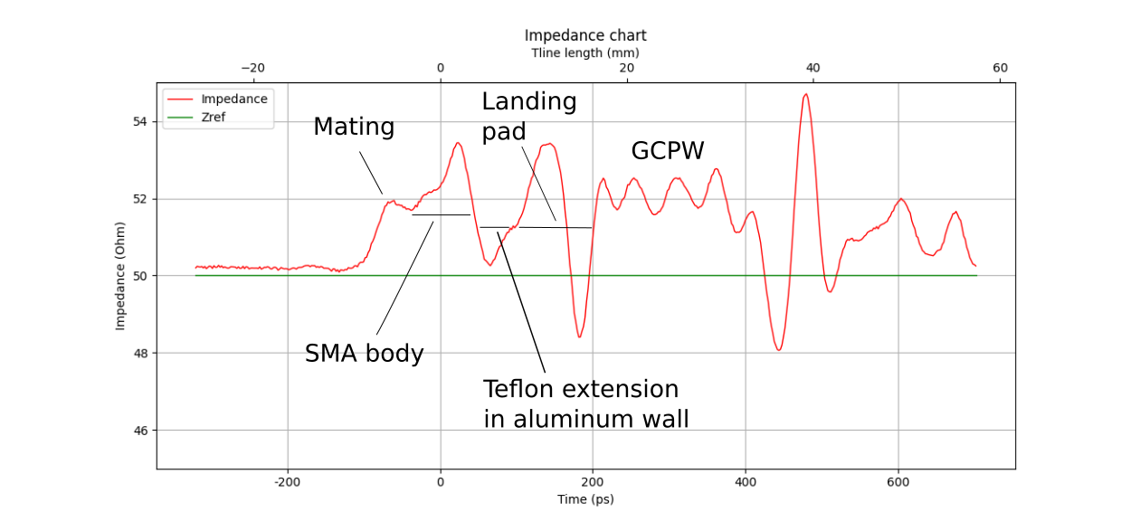
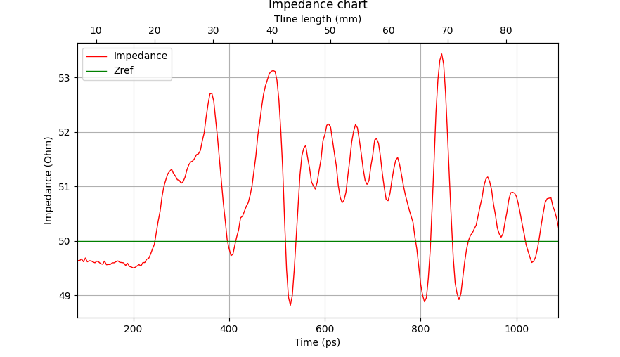
The reflections caused by the above transitions will be quite small. The signal travels through all these coaxial segments as a TEM wave, so there is no change in the electric or magnetic field orientation. The impedances of all individual segments will also differ only slightly. These discontinuities, although small, will be visible in the TDR trace as deviations from the characteristic impedance (Figure 3).
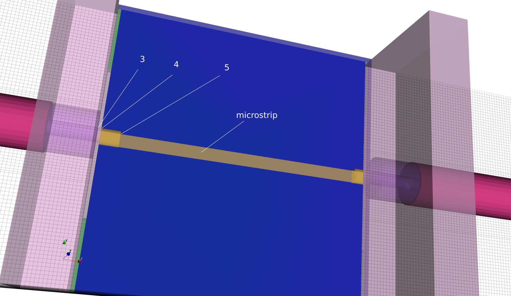
The next transitions are the most challenging to control. The first in this series starts where the contact pin of the SMA connector leaves the aluminum wall ('3') and ends where it touches the copper landing pad on the circuit board ('4'). In other words, there is a (small) gap between the aluminum wall and the circuit board (remember we are using a panel mounted connector). In theory this distance can be close to zero, but in practice there will be a difference due to PCB size tolerances. Also, the copper pad on the circuit board often does not end perfectly on the edge of the circuit board. So we should model it. Either as a very short transmission line, or as an LC (lowpass) network. In most cases it is not easy to find the right parameters for this segment. Again, a TDR trace is useful because it shows the gap as an impedance spike. But if the TDR bandwidth is limited (or the gap is very small compared to the wavelength), you won't find it in the TDR trace.
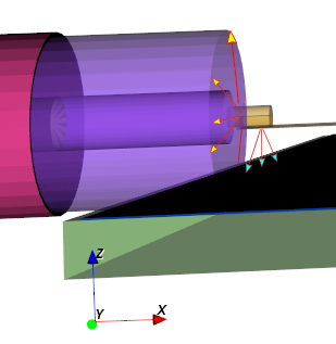
Once the signal has passed through the gap, it enters the landing pad area ('4'). This segment can be modeled as a microstrip or as a grounded coplaner waveguide ('4'-'5'). This transition brings many changes to the RF signal. First, there will be some impedance discontinuity at the segment boundaries. Second, the E and H field lines change direction to align with the new configuration of conductors (Figure 4). The return current path also changes, from a coaxial distribution to a planar-plane distribution. The design of the PCB landing pad and the construction of the RF enclosure play an important role in this transition.
Finally, the SMA landing pad connects to a GCPW ('6') in this example. There is often an additional transition after the SMA landing pad. For example, if you need to connect to a microstrip after the GCPW landing platform.
By dividing the signal path in multiple transmission line segments, it becomes easier to design a system that minimizes reflections. The design task now is to hold the impedance of each segment as close to the target characteristic impedance as possible and to create smooth transitions between them. This approach is used in the next two paragraphs.
Dividing the signal path into multiple transmission line segments makes it easier to design a system that minimizes reflections. The design task is then to keep the impedance of each segment as close as possible to the target characteristic impedance and to create smooth transitions between the sections. This approach is used in the next two sections.
2. SMA Landing Pad Design Examples
In this section we show two design examples. One for a simple microstrip design using the RF-ENCL-MINI as an enclosure and another, more advanced design with a 4-layer PCB mounted in an RF-ENCL-MINI-EXT-FX enclosure. The latter also shows how to design a transition from GCPW to microstrip.
2.1 Example of a microstrip landing pad, two layer PCB
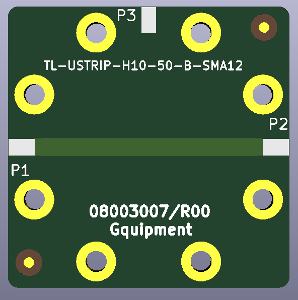
The design goal is to create a coax-to-microstrip transition with a maximum return loss of -20 dB over a frequency range of 18 GHz. The PCB has a relative dielectric constant of 4.5. We use an RF-ENCL-MINI that supports a 26.8 x 26.8 mm PCB.
- Use a PCB with a substrate height of 1.0 mm
- Make an initial design using an impedance calculator
- Reduce the impedance of the SMA pad by a few ohms
- Use a 3D EM solver to model and simulate the configuration.
- Build it and measure the return loss and a TDR trace. Use the TDR trace to improve where necessary.
Figure 7 gives a good overview of what this configuration looks like, including the connector, housing, and landing pattern. Figure 8 shows the TDR trace for this configuration. As expected, the transitions from 1) to 3) do not cause many problems. The air gap ('3'-'4') is designed to be (maximum) 0.1mm to account for PCB size tolerance. If this gap is too large (several tenths of a mm), the TDR trace will reveal an impedance peak at this position.
Then follows the SMA connector pad ('4'). It just has a rectangular shape. Impedance can be calculated using one of several microstrip line calculators, all of which provide an accurate prediction of the expected impedance. However, keep in mind that there is also a contact pin above the pad and some solder as well. This increases the capacitance of the pad, meaning the impedance will be a few ohms lower than expected. There are various options to compensate for this dip. We can make a smaller pad, increase the height between the pad and the ground plane, or use a substrate with a smaller dielectric constant. In this design we reduced the pad width by 0.1mm.
The TDR trace shows that the impedance is still 1 ohm lower than the characteristic impedance (50 ohms). It is possible to eliminate this small impedance drop by making a small recess in the ground plane of the circuit board under the connector pad. This lowers the impedance because there is a small air pocket in the aluminum mounting edge of the housing. It's there on purpose and the effect is that you can increase the height between the pad and the ground plane, increasing the impedance. However, in this design we have not used this option.
Also note that the housing is optimized for a PCB substrate height of 1.0mm. In that case, the contact pin just touches the copper connector pad. This creates a smooth transition in the Z direction. Additionally, the 1.0mm is a good starting point if you are working with a relative dielectric of 4.5. Using lower dielectric constant substrates is not a problem (FR408, RO6003C), just increase the path and signal linewidth to compensate for the lower capacitance.
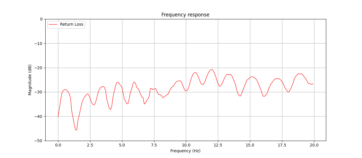
2.2 Interpreting the return loss chart
The return loss diagram is shown in Figure 9. Note that this is the return loss of the microstrip terminated at both ends with an SMA connector. So what the graph actually shows is the result of the reflections at both SMA connector transitions interfering with each other. The number of peaks and valleys is a function of the length of the microstrip (including the connectors) and does not have much to do with the magnitude of the reflections at the connector transitions. The peaks occur where the reflections are in phase (at the reference plane). The valleys form where the reflections cancel each other out, as if there were no reflections at all.
If you only want to see the return loss caused by the transitions of a single SMA connector, some form of windowing technique must be applied to the TDR trace to isolate its reflections. The return loss can then be calculated using an FFT. The graph would then not show the impedance peaks and valleys, because constructive and destructive interference can no longer occur. The resulting retrun loss diagram would then be much more of a smooth line a few dB below the peaks shown in figure 9.
2.3 Example of a GCPW landing pad, four layer PCB
The next example uses a four-layer printed circuit board (Figure 11). It implements a microstrip using layers 1 and 2 (the top two layers), while the SMA landing pad has a GCPW design using layers 1 and 3 (layer 4 is the bottom). The printed circuit board has a thickness of 1.6 mm. The distance between the two top layers and the bottom two is 0.2 mm FR408 (Er of 3.65). The core between layers 2 and 3 is 1.2 mm.
We use the RF-ENCL-MINI-EXT-FX as an enclosure (Figure 10). The advantage of this enclosure is that it supports any PCB thickness between 0 and 1.6mm due to the unique way the PCB attaches to the mounting points. Additionally, the PCB mounting points provide a current return path on both the top and bottom layers of the PCB (just as an edge-mounted connector would). So we have the benefits of an edge connector type connection, while remaining flexible with respect to the thickness of the PCB.
- Create the microstrip connecting the two SMA landing pads using layers 1 and 2 and use an impedance calculator. The calculated trace width should work well in practice.
- Use a GCPW design with layers 1 and 3 for the landing pad and again use a calculator to find the dimensions. Start at a target impedance of 50 ohm. It is important to create a large cutout area in layer 2, otherwise this structure would have far too much capacitance.
- Use vias as you would in a GCPW.
- Make a transition between the GCPW (L1, L3) and the microstrip (L1, L2). It is important that there are vias at both sides of the GCPW connecting layers L1 and L2. Because that creates a short path for the return currents between the GCPW (L1 ground planes) and the microstrip (L2 ground plane).
- Start with an 'abrupt' transition: the microstrip starts exactly where the GCPW ends. You can further enhance this transition by applying tapering in the signal trace and the cutout area in layer 2 to create a smooth transition.
- Use a 3D EM solver to model and simulate the configuration. An EM solver is more or less required to determine the exact tapering.
- Build it and measure the return loss and a TDR trace. Use the TDR trace to improve where necessary.
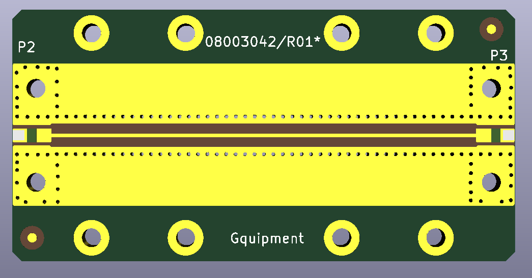
In figure 12 you can see how the landing pattern looks like and figure 13 shows the TDR trace. Once again, its starts getting interesting at position '4' where the connector pin leaves the wall of the enclosure. Again, there is an air gab between the edge of the PCB and the wall of the enclosure. The connector pin of the SMA connector that comes with the enclosure has a diameter of only 0.5 mm. This causes a strong impedance peak at this position. That is easily remedied by soldering the connector pin up to the base of the connector. This creates a smooth transition bridging the air gab ('3'-'4'). The pad which is designed as a GCPW is easily identified with its transition to the microstrip. Also note the cutout in layer 2 to prevent a otherwise much to high capacitance below the relatively large solder pad.
In figure 12 you can see what the landing pattern looks like and figure 13 shows the TDR trace. Once again things get interesting at position '4', where the connector pin leaves the wall of the housing. Here too, there is an air gap between the edge of the printed circuit board and the wall of the housing. The connector pin of the SMA connector supplied with the housing has a diameter of only 0.5 mm. This causes a strong impedance peak at this position. This can easily be resolved by soldering the connector pin to the connector base. This creates a smooth transition that bridges the air gap ('3'-'4'). The pad designed as a GCPW is easy to recognize including the transition to the microstrip. Also pay attention to the cutout area in layer 2 so that the capacitance under the relatively large soldering surface does not become too high.
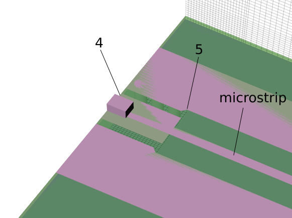
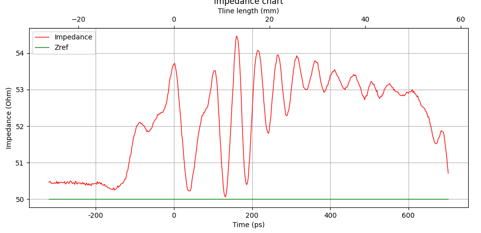
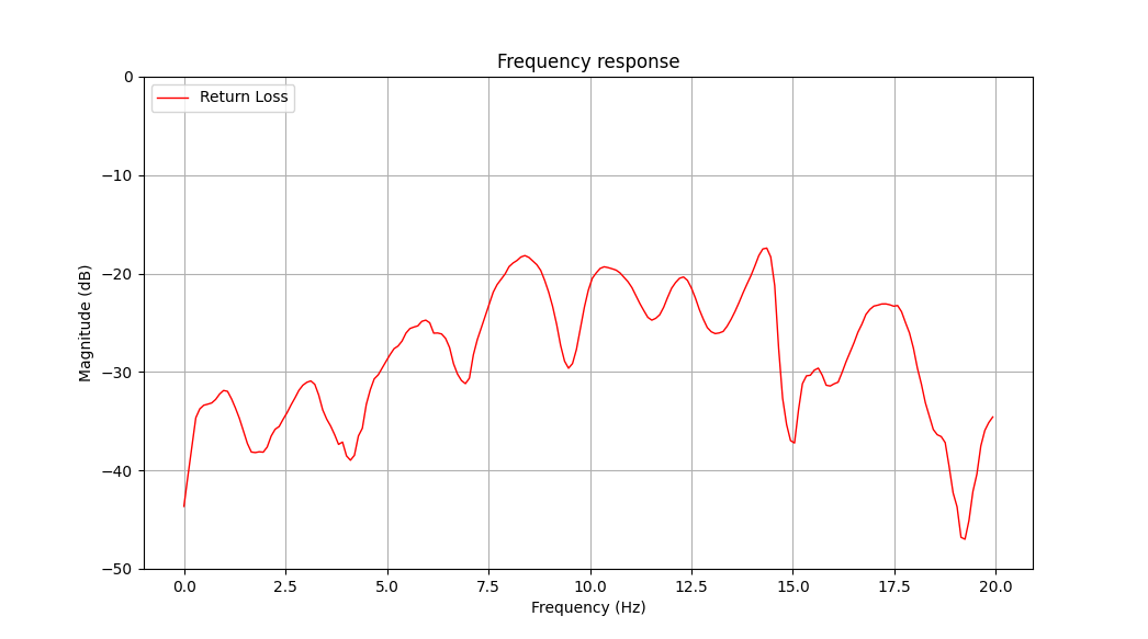
Figure 14 shows the return loss graph up to 20 GHz. The return loss remains below -20 dB over the entire frequency range. As mentioned in the previous case, the peaks and valleys in the return loss graph are created by the interference between the reflected signals on both SMA ports, as seen from one of them. The peaks are where the reflections are in phase and the valleys are where they cancel each other out. The contribution of a single SMA connector with its landing pad is a few dB lower than the peaks in this graph.
3. Reference designs
To assist the RF engineer, the RF-ENCL-MINI series comes with reference designs. They are described in an application note, while the PCB gerber files can be found on Github. It gives the designer a quick start and saves time. There are reference designs for both microstrip and GCPW transmission lines. For your convenience, please find the links below:
RF-ENCL-MINI (PCB of approx. 1x1 inch):
RF-ENCL-MINI-EXT-FX (PCB of approx. 2x1 inch):
4. General Guidelines
We conclude this article with a summary of best practices you can use when designing a low return loss SMA pad.
- Keep air gaps at the edge of the PCB as small as possible. Also eliminate the copper clearance at the edge of the board as this has a similar effect.
- Treat the design problem as a sequence of several transmission line segments.
- Tune the impedance of the SMA landing pad by changing the distance between the pad and the groundplane between (top layer / groundplane) and/or by adjusting the gab between signal and ground strips on the (same) top layer (GCPW configuration only).
- Make sure that their is a short path for the return currents. This is especially important if there is a change of ground plane layers.
- Use tapering to create a smooth transition at the segment boundaries. Use a 3D EM solver to simulate the exact shape of the tapers.
If you have any questions or remarks, please feel free to contact us.