Bias tee applications
A bias tee (aka Bias-T) is a versatile device that can be found in many applications. Its primary function is to inject a DC bias voltage into a coaxial RF link. This link can then be used to simultaneously transfer both an RF signal and power to an RF module. There are three common use cases for a Bias-T that each solve a different problem:
- To power an remote amplifier. Typically an LNA in an antenna system. The goal here is to improve the S/N ratio as much as possible directly at the antenna, while avoiding the use of additional cabling to power the LNA.
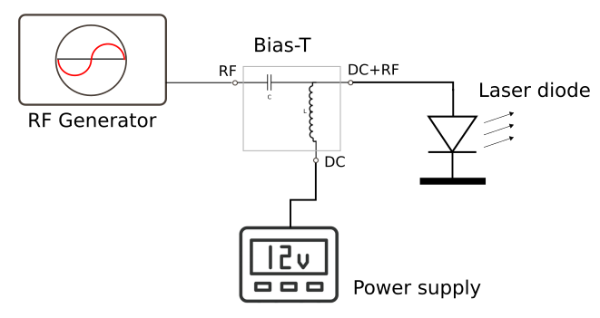
- To bias a laser diode. A laser diode is a single-port device, so DC bias and the RF signal must be supplied over the same RF link. This is a natural fit for a Bias-T
- To measure the RF characteristics of an active discrete RF component, such as a BJT. The measurement is usually done with a VNA. Bias-Ts are used to inject a DC voltage into each of the RF measurement ports to bias the BJT. Note that a fixture is required to connect the BJT pads to the coaxial connectors of the measurement system.
In this article, we will look at these three examples. We also did some lab experiments to demonstrate the BJT biasing use case. But before we go to the examples, let's first study the Bias-T itself.
1. What does a Bias-T do?
The basic operation of a Bias-T can be explained by looking at its circuit diagram (Fig. 1). It consists of only an inductor and a capacitor. A DC voltage applied to port 3 passes through the inductor without attenuation and reaches port 2. At the same time, an RF signal applied to port 1 passes through the capacitor without attenuation and also reaches port 2, together with the DC voltage. In this way, the Bias-T is used to combine a DC voltage (bias) with an RF signal and thus feed an RF link (such as a coaxial cable).
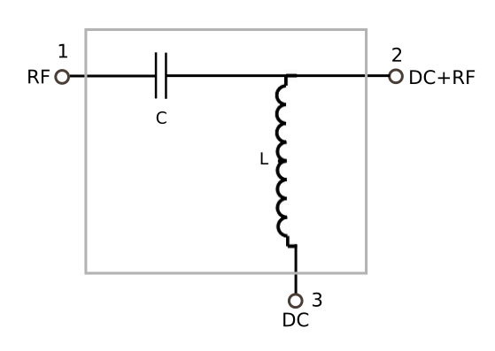
Also, the capacitor acts as a DC block. So the voltage applied to port 3 is isolated from port 1. Similarly, the inductor isolates the RF port (1) from the DC port (3).
The Bias-T is a reciprocal device, so it can (and is) also used to separate the DC and RF components present on port 2. The example in section 2 shows an example where the Bias-T is used in both ways to power a remote LNA.
It helps to think of a Bias-T as a diplexer. A diplexer is a device that splits an RF signal into two separate frequency bands. In this case, the inductor acts as a low-pass filter (DC path) and the capacitor acts as a high-pass filter (RF path).
In practice, a Bias-T has some limitations because capacitors and inductors are not ideal components. Especially the inductor limits the frequency range at both the lower and upper end. The lower end is determined by the limited inductance and the upper end is caused by the parasitic capacitance of the inductor.
For these reasons, in a practical wideband Bias-T, great care is taken to design a suitable inductor. One solution is to use a conical inductor. This type of inductor has a high inductance, while keeping the parasitic capacitance under control by making the windings a little smaller with each turn. The disadvantage is that it is not very production-friendly.
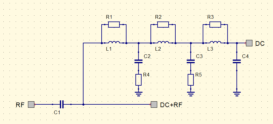
The other solution is to use multiple inductors in series with decreasing inductance as they get closer to port 2 (RF+DC). These inductors have progressively higher self-resonance (i.e. lower parasitic capacitance). In this way, adequate isolation can be achieved well into the GHz range. An example of such a construction is shown in figure 2. The schematic shows that the inductors are surrounded by resistors and capacitors to control the resonance effects created by the inductors. Without these additional components, peaks and valleys would occur in the S-parameters of the device.
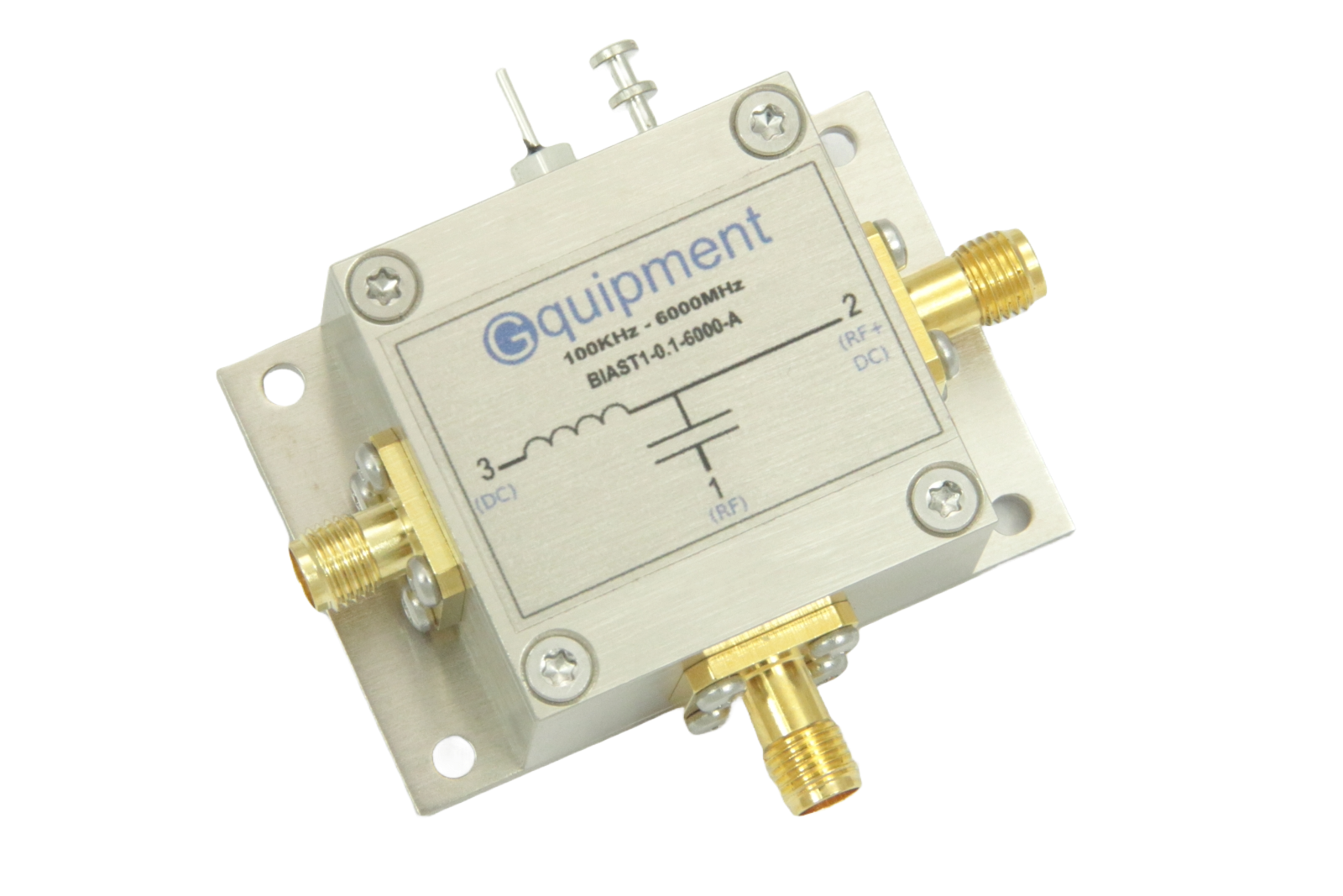
The BIAS-T1-0.1-6000-A-YF is an example of a Bias-T with a frequency range of 100kHz to 6 GHz by using 4 segments.
1.2 What Are the Relevant Bias-T Parameters?
When selecting a Bias-T, you should consider the following parameters.
Bandwidth
The bandwidth of a Bias-T is the frequency range where the insertion loss stays within 3 dB while maintaining adequate isolation and return loss at its RF-carrying ports.
Insertion loss
This defines the loss of power in the RF path (S21). Ideally, it should be as close to 0 dB as possible.
Isolation
The attenuation between the DC port (3) and one of the RF carrying ports (1, 2) is called isolation (S31, S32). The higher the isolation, the better. Isolation should be at least 20 dB.
Return loss
The RF ports (1 and 2) should match the characteristic impedance they are designed for (usually 50 ohms) to prevent unwanted reflections at the RF ports. A return loss value of 15 dB is acceptable, while 20 dB or higher is considered very good.
Max Voltage
This is the maximum voltage that can be applied to one of the RF ports without damaging the device. This limit is set by the type of capacitor used in the Bias-T.
Max DC current
This is the maximum DC current that can flow between the DC port and the (DC+RF) port. A higher current will damage the device. The inductor(s) determine the upper current limit.
Max RF power
The maximum RF power that can pass between the RF and (DC+RF) ports without damaging the device.
2 Examples of Common Bias-T Uses Cases
In this chapter we discuss three common applications in which the Bias-T plays an important role.
2.1 Powering a (remote) LNA with a Bias-T
A common use of a bias-T is to power an LNA that amplifies the signal from an antenna. Often the coaxial cable between the antenna and the receiver is quite long. This is a problem because a long cable will heavily attenuate RF signals. This will degrade the S/N ratio. For this reason, an LNA is used at the antenna side to amplify the signal to overcome the cable attenuation.
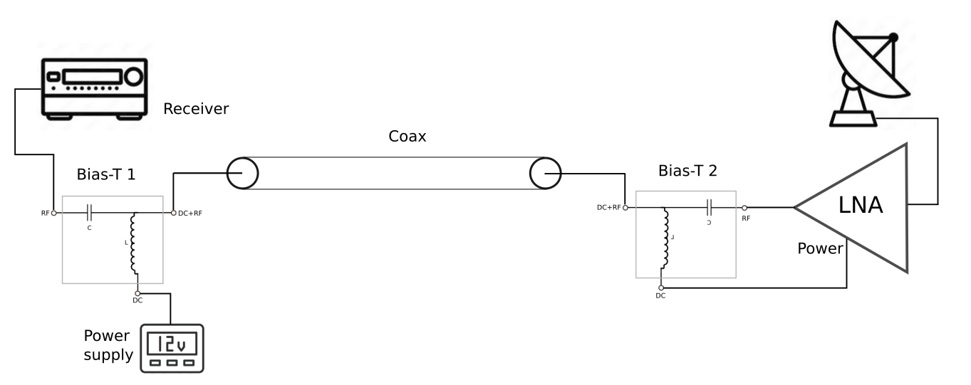
In such a situation, a Bias-T is a convenient solution to supply power to the remote LNA by using the existing coaxial cable. Figure 3 shows how this can be achieved by using two Bias-T's. The first, on the receiver side, is used to supply power (by applying a DC voltage) over the coaxial connection while passing the RF signals to the receiver. On the antenna side, the reverse happens: the Bias-T supplies the DC voltage to the LNA and isolates it from the amplified RF signal which is fed on the coaxial cable.
Often the LNA is accompanied by a mixer to convert the RF signal back to a lower frequency, because the attenuation in an RF cable increases with frequency.
2.2 Using a Bias-T to Modulate a Laser Diode
There are many ways to bias and modulate a laser diode. One of them is by using a Bias-T. It is an obvious solution because the laser diode is a single-port device that needs to be powered by both an RF signal and a DC voltage to bias the diode. A typical circuit diagram is shown in Figure 4. The selected bias voltage determines how the laser diode is operated: either in its linear region or at its on/off threshold. The former method is used to modulate in an analog style, while the latter is used to produce a digital output.
2.3 Using a Bias-T to Measure the S-parameters of a BJT
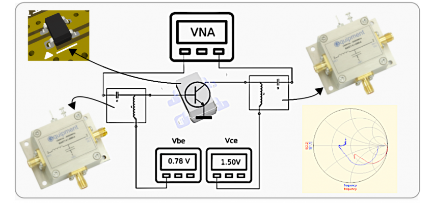
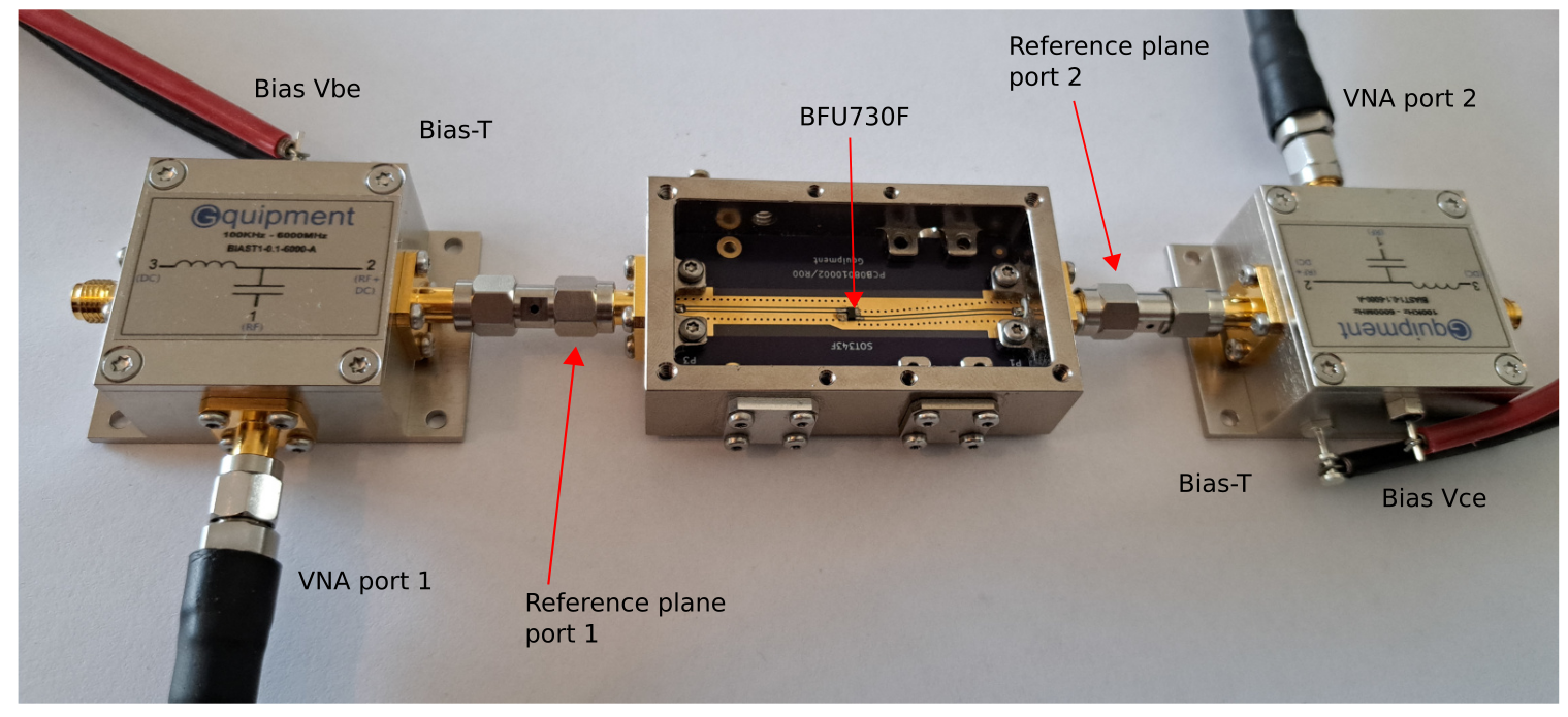
To measure the S-parameters of an active component such as a BJT, it must be properly biased. Although a BJT has 3 terminals, the S-parameter measurement involves only two RF ports, as explained in section 5.1 of this article. Both RF ports must provide a DC voltage to bias the BJT into the desired operating range. This can be accomplished by using two Bias-T's. A typical test setup is shown in Figure 5. Note that in addition to the Bias-T's, some form of fixture is also required to connect the coaxial ports to the terminals of the BJT. In this example, a test enclosure with two RF ports and a PCB with a SOT343F footprint is used.
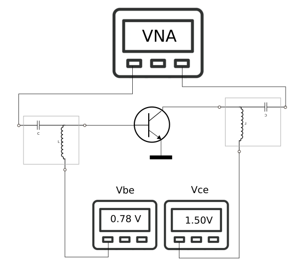
We used this setup to measure the S-parameters of a NXP BFU730F transistor. The VNA was calibrated with the Bias-Ts installed. Fixture effects were removed by applying de-embedding. Measurements were made for various values of Vce and Ic. These were set by adjusting both Vbe and Vce with a lab power supply. The power supply should be able to accurately adjust the voltage between 0 and 3 volts, in 0.01 volt steps, especially for Vbe. Additionally, a current limiter is nice so that you can safely experiment with the biasing of the BJT without worrying about blowing the component up. We set the current limit for Vce (aka Ic) to 30 mA. Also note that the Vce limit is only 2.8 volts for the BFU730F.
Make sure the output power of the BJT does not exceed the input port limit of your VNA. The BFU730F has a lot of gain in the lower frequency range! Also make sure you do not drive the BJT into saturation, as this will distort the S-parameter measurement. The default configuration of a VNA will probably need to be modified to accommodate this. We configured our VNA to apply 30 dB of attenuation to port 1.
The selected Bias-T (BIAS-T1-0.1-6000-A-YF) is a wideband device that can be used between 100 kHz and 6 GHz. Picture 1 shows what it all looks like.
Bill of Material
- BJT: BFU730F by NXP, SOT343F. Datasheet
- Bias-T: BIAS-T1-0.1-6000-A-YF
- Fixture : RF-ENCL-MINI-EXT-FX-YF-01
- PCB : 08010002/R00
Once the measurement setup is finished, it is straightforward to measure the S-parameters at different bias conditions. We took 5 measurements starting at Ic=5mA and Vce=1V and step wise increased both Vce and Ic. We stopped at Vce=2.5V and Ic=25mA. We also checked our measured data with the S-parameters published by NXP which correspond well. The only deviations we discovered are in the return loss traces for the Ic>15mA condition. They reveil a lambda/2 resonance at 3.5 GHz which corresponds with the length of the coplaner transmission lines of the PCB. Therefore, a smaller fixture would have been beneficial, for example, the RF-ENCL-MINI-YF-01, which is a factor 2 smaller, would have moved this resonance practically out of band (to 6 GHz).
Once the measurement setup is complete, it is easy to measure the S-parameters at different bias conditions. We did 5 measurements, starting at Ic=5mA and Vce=1V and incrementally increasing both Vce and Ic. We stopped at Vce=2.5V and Ic=25mA. We also checked our measurement data with the S-parameters published by NXP and they agree well. The only deviations we found are in the return loss traces for Ic>15mA. They reveal a lambda/2 resonance at 3.5GHz, which corresponds to the length of the coplaner transmission lines of the PCB. Therefore, a smaller fixture would have been beneficial. For example, with the RF-ENCL-MINI-YF-01, which is a factor 2 smaller, this resonance would have been practically out of band (6GHz).
In the following figures we show the S-parameter graphs for 1V-1mA, 1.5V-5mA and 2V-20mA. You can clearly see that more current significantly improves the high frequency gain and return loss figures. It is also worth studying the Smith charts, which are very useful when designing an impedance matching network for this BJT. The graphs also show that in practice impedance matching will be necessary. As you would expect for this type of RF transistors.
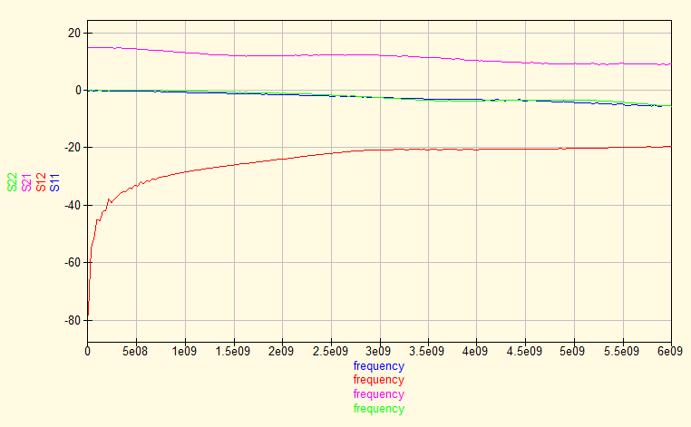
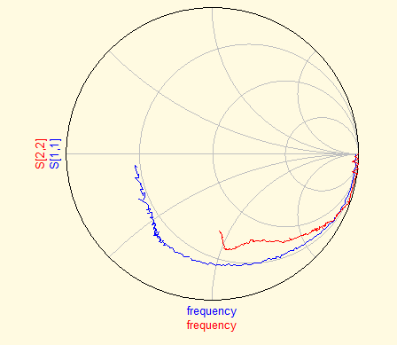
Figure 8: Smith chart at VC=1V and Ic=1mA
Figure 7 shows that at Vce=1V and Ic=1mA the BFU730F reaches its usable operating range. However, the gain is still modest and the return loss is really bad. Also don't expect good IP3 figures at such a low collector current. The Smith chart shows that the input and output impedances are mainly capacitive.
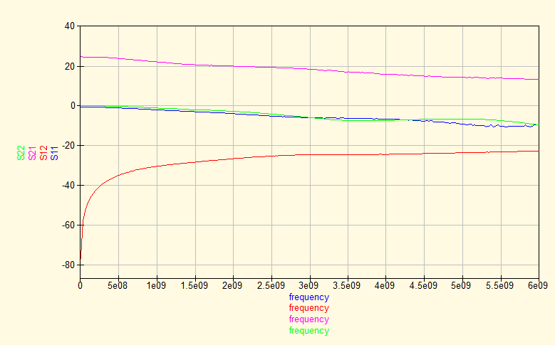
Figure 9: S-parameters at VC=1.5V and Ic=5mA
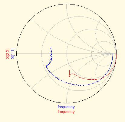
Figure 10: Smith Chart at VC=1.5V and Ic=5mA
Setting the BFU730F to Ic=5mA and Vce=1.5V improves all parameters: we get (much) more gain, better isolation and the input and output return loss improves over a wide frequency range. Increasing Vce further to 2V and Ic to 20mA improves the gain even further, but only for frequencies <3GHz, while the return loss figures, again, improve over the full frequency range.
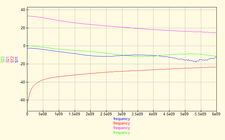
Figure 11: S-parameters at VC=2V and Ic=20mA
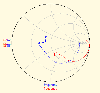
Figure 12: Smith Chart at VC=2V and Ic=20mA
These types of measurements are the first step in applying a BJT as an RF amplifier. The next steps would include adding the appropriate bias and impedance matching circuits. Also, some feedback would be useful for both stabilizing the operating point and smoothing the frequency response of the amplifier.
3. Concluding Remarks
In addition to the three applications mentioned above, we have also seen Bias-Ts in places where you might not immediately expect them. The first is to use the RF path only, as a replacement for a DC block. The other is the exact opposite: use the DC-to-RF port (the path containing the inductive element) to filter the output of a power supply. These use cases show that a Bias-T is a versatile device in your RF lab. Especially the wideband kind due to its wide application range.
