A bias tee (aka Bias-T) is a versatile device that can be found in many applications. Its primary function is to inject a DC bias voltage into a coaxial RF link. This link can then be used to simultaneously transfer both an RF signal and power to an RF module. There are three common use cases for a Bias-T that each solve a different problem:
To power an remote amplifier. Typically an LNA in an antenna system. The goal here is to improve the S/N ratio as much as possible directly at the antenna, while avo [...]
Read more >
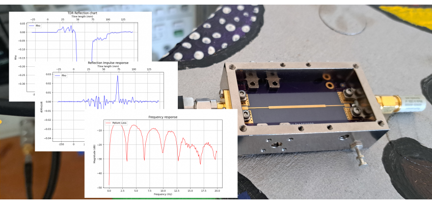
In this article, we explain how to transform a time domain TDR (Time Domain Reflectometry) measurement into a frequency domain return loss graph. Since the TDR trace is in the time domain and the return loss (S11) is in the frequency domain, an FFT is used to perform the transformation. The steps are implemented using a Python script. The article concludes with some examples of different DUTs.
1. Why transform a TDR trace to return loss (S11)?
Before we answer this question, it's a good idea to summarize [...]
Read more >
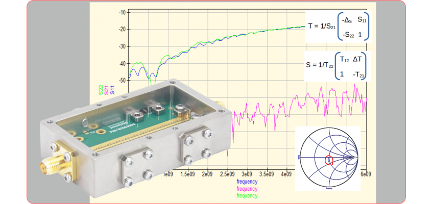
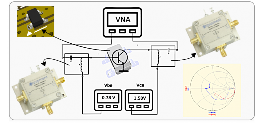
Performing S-parameter measurements on RF components can be quite challenging. The problem arises from the fact that the connections of typical RF components, for example SMD components, cannot be connected directly to a VNA because, of course, they do not have coaxial connectors. Therefore, some type of fixture is needed that houses the SMD part and connects it to coaxial connectors (Picture 1). However, this fixture with its connectors and 'wiring' will affect, often seriously, the measurement of the RF p [...]
Read more >
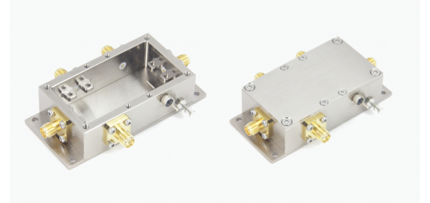
The RF Enclosure MINI-EXT-FX is a new line of RF enclosures that speed up your RF development project by creating housing, high-performance SMA ports, RF grounding, and thermal stability all in one go. Best of all, replacing the PCB with a new revision is easy, so the enclosure can be reused for your next project.
The RF MINI-EXT-FX can be conveniently used in small-series production.
The EXT designation refers to the doubled length of the PCB that fits in the enclosure, compared to the MINI version. The [...]
Read more >
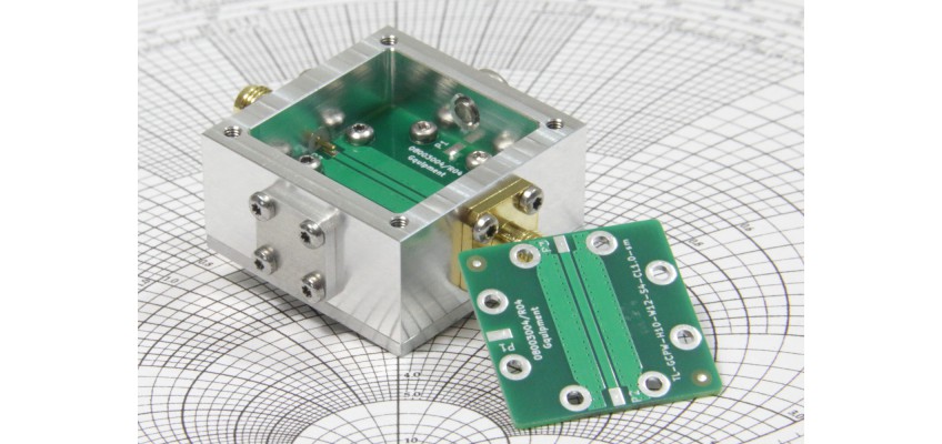
A common problem with almost any RF design is how to make a good connection between the coaxial connector and a signal trace on the circuit board. Several impedance transitions and/or changes in direction of the EM field play a role here, which cause unwanted reflections that disrupt and distort the signal. In general, this phenomenon already starts to play a role at frequencies above 1 GHz. The amount of signal reflection is expressed as Voltage Standing Wave Ratio (VSWR) or return loss (RL). In this artic [...]
Read more >
 A bias tee (aka Bias-T) is a versatile device that can be found in many applications. Its primary function is to inject a DC bias voltage into a coaxial RF link. This link can then be used to simultaneously transfer both an RF signal and power to an RF module. There are three common use cases for a Bias-T that each solve a different problem:
To power an remote amplifier. Typically an LNA in an antenna system. The goal here is to improve the S/N ratio as much as possible directly at the antenna, while avo [...]
Read more >
A bias tee (aka Bias-T) is a versatile device that can be found in many applications. Its primary function is to inject a DC bias voltage into a coaxial RF link. This link can then be used to simultaneously transfer both an RF signal and power to an RF module. There are three common use cases for a Bias-T that each solve a different problem:
To power an remote amplifier. Typically an LNA in an antenna system. The goal here is to improve the S/N ratio as much as possible directly at the antenna, while avo [...]
Read more >