Modeling Devices with S-parameters
Scattering parameters or S-parameters for short, are the standard way to describe the behaviour of all kind of RF modules. Both passive and active. So, what are these parameters and why are they so popular? In order to fully grasp the full potential of S -parameters, it is useful to lay down some basic concepts first.
(Note: some understanding of transmission line theory is helpful when reading this article)
1. S-parameter basics
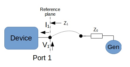
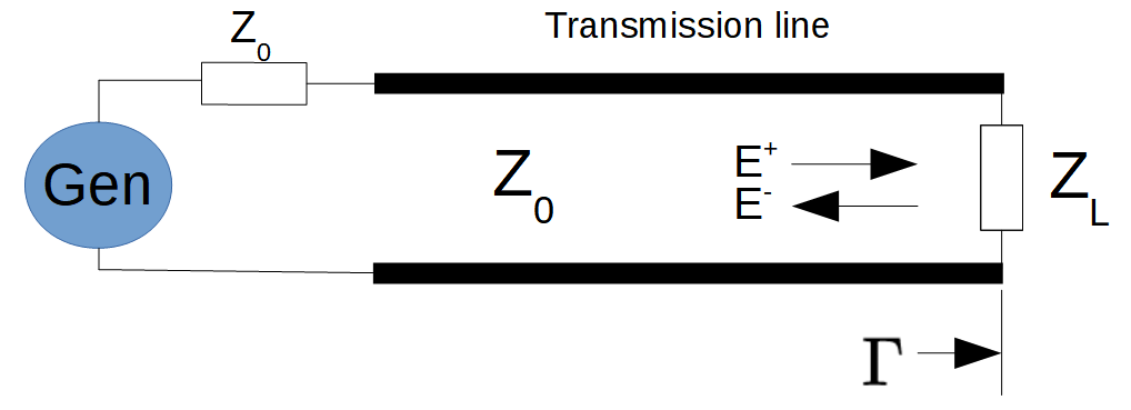
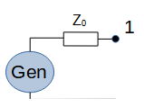
The basic idea behind S-parameters is to look at a device (or more generally, a network) as a black box. Where only the input and output ports can be interacted with. Each port has an impedance (‘Zx’) associated with it. We can also apply a voltage (V1) that causes a current (I1) to flow. It is essential for the definition of S-parameters that each port 'sees' a impedance Z0. So when a generator powers a port, it must have an impedance of Z0. Usually, Z0 is equal to 50 or 75 ohm. Z0 is also called the reference impedance of the system.
The next important concept is that we are always talking about (power) waves that travel through these ports. Power waves can both enter or exit a port. Because we are talking about traveling waves, transmission line theory must be applied.
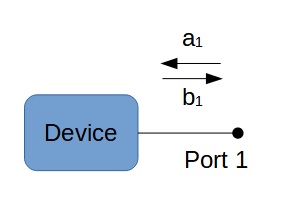
The S-parameter universe is defined around the power waves that are incident to a port (‘a’) or that leave a port ('b'), instead of talking about voltages and currents.
If we connect a transmission line (for example: a coaxial cable) to a port and the impedance of the port and the transmission line are exactly matched, all power will be transferred to the port. However, if there is a mismatch, then there will be some power reflected back into the line.
Finally, we need to introduce the reference plane (Figure 1). The importance of the reference plane becomes apparent when one realizes that a transmission line changes the impedance and phase of the power waves as a function of its position on the line. Thus, all ports related to S parameters are positioned on their reference plane. S-parameters are only valid on their reference plane. Sometimes one wants to measure an element that is some distance from the measuring port. In that case, various de-embedding techniques exist to move the reference plane to the element of interest, without changing the position of the measurement port.
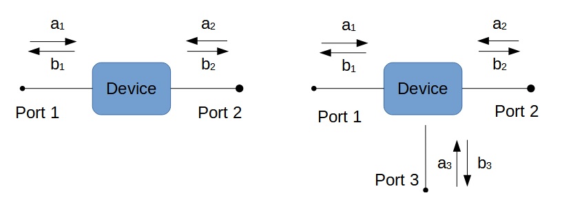
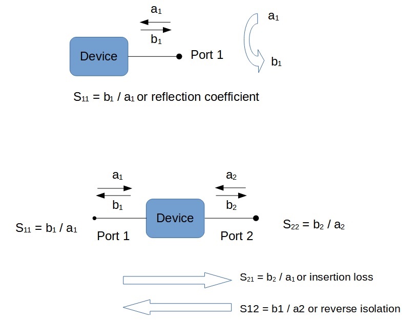
In this section we’ve restricted ourselves to a one-port device so far. Of course, there are devices with more then one port too! In general, a device can have ‘N’ ports. In the following figure an example is given of a two- and three- port device.
A good example of a one-port device is a 50 Ohm terminator or an antenna. An attenuator or a filter are exemplary for two-port devices. While a power splitter can be modeled as a three-port device.
1.1 S-parameters and Their Physical Representation
Now we are ready to explain what a S-parameter is and what it means. An S-parameter of a device is a ratio between the (power) waves at and between its ports. As there are both incident- and reflected- waves and one or more ports, it follows that a device in general will have many S-parameters to model its behaviour.
We will break this down for a one-, two- and three- port device.
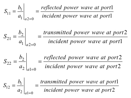
With a one-port device there is no ratio of power waves between its port as there is only one port. That leaves us with the only ratio that does exist - the ratio between the reflected power versus the incident power wave. That is the ratio b1 / a1, and is denoted with S11. This is called the reflection coefficient or return loss. Which is also the physical manifestation of S11.
Next is the two-port devices. Our first observation is that for each individual port there is an S11 and an S22 reflections coefficient. But now there are also power wave ratio's possible between ports 1 and 2. The first one is the relation S21 which is defined as the power wave ratio of b2/a1 (while keeping a2 at zero so that b2 is merely accounted for by a1). The name of this parameter (S21) is insertion loss. Again, this is a good way to describe its physical expression when the two-port device is a cable or some sort of attenuator. If the device is an amplifier, gain is the preferred name of S21.
The second port-to-port relation is S12 , which equals b1/a2. This is the ratio of the incident wave at port 2 and the power wave leaving port 1 (while keeping a1 at zero). The name of S12 is reverse isolation. It can be shown that for a reciprocal device S21 and S12 are always equal (most passive devices are reciprocal). Which intuitively makes sense, since the insertion loss and the reverse isolation of a cable will clearly be the same. However, if we look at an amplifier, gain and reverse isolation will most likely be different and here the meaning of reverse isolation is self- explanatory.
In the next figure you will find a summary of the three types of S-parameters we looked at so far.
In this section the emphasis is on the physical meaning of S-parameters. Which depends on the context the device is used in. The S-parameters are always just a ratio of two power waves. We will finish this paragraph with another example of the meaning of S-parameters by looking at a three port device: the power combiner (see figure below).
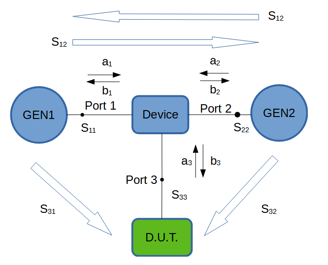
The function of a power combiner is to combine the power waves from the generators GEN1 and GEN2. This is a quite common test setup for performing Inter Modulation Distortion (IMD) measurements. The D.U.T. could be some sort of amplifier. In this context it is important that both signals are equally added and fed to the D.U.T. So S31 must equal S32. The second concern in this type of measurement setup is that GEN1 does not influence GEN2 and vice versa. They are typically operated at frequencies that are very close together. So S12 and S21 should be as small as possible. Note that they will also be equal as a combiner is a passive device. In this situation, S21 and S12 are called the isolation parameters of the device. For these types of measurements, an splitter with an isolation of 20dB or higher is recommended.
1.2 Frequency-dependent
Devices described by S-parameters often show some sort of frequency-dependent behaviour. For example the device should pass low frequencies only. Or, alternatively, they are designed to do something which should be as frequency-independent as possible. As is the case with an attenuator or amplifier. In either case, we are always interested in the S-parameters for a frequency range of interest. S-parameters are therefore mainly presented in graphical or tabular form.
1.3 Linear Systems Only
Please note that S-parameters only apply to linear systems. When a set of S-parameters is given for a non linear device such as a BJT transistor, it will be valid for small signal analyses only.
1.4 Amplitude and Phase
When modeling the properties of a device (like insertion loss or gain), we are generally interested in both the magnitude and phase information of the transfer function. Therefore, S-parameters are complex numbers that model both these properties. The same goes for other quantities like Z, V, I or the reflection coefficient Γ. Because the phase must be known, S-parameters can only be measured with an Vector Network Analyzer (VNA) and not with a Spectrum Analyzer (SA).
1.5 Origin of the term 'Scattering'
The name 'scattering' is taken from the optical field where it is used to describe how an EM wave behaves as it passes through different media. Similar to an RF power wave passing through an impedance discontinuity, causing the wave to be 'scattered'.
2. S-parameter Definitions
In this section we will take a more formal and general approach to the description of devices by means of S-parameters. The purpose is not to give an elaborate treatment of the subject-matter, but to point out some important issues that (hopefully) will assist you when working with S-parameters.
2.1 Notation and Definitions
The relations between the power waves from figure 4 (ax and bx) can be written down in the following equations:
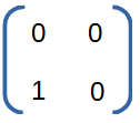
b1 = S11 . a1 + S12 . a2
b2 = S21 . a1 + S22 . a2
These type of linear equations lend themselves well to writing down in vector notation. This will prove quite handy when we are working with devices with more than two ports.
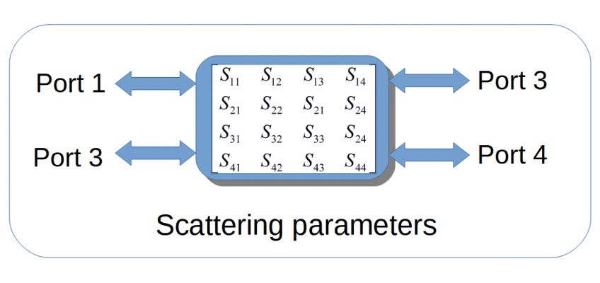
So, b = S . a, with the vectors a and b containing the successive power waves 'ax' and 'bx'. S is the matrix containing all the S-parameters.
For the set of equations above, S looks like:

The formal definitions of the S-parameters are:
2.2 What About that Power Wave?
In the definitions above and in paragraph 1, we already talked about power waves 'a' and 'b'. However, this was done without a proper introduction. We will now take a closer look at this phenomenon, but without the mathematical treatment.
We start the discussion by introducing the definitions of both 'a' and 'b' for a port:
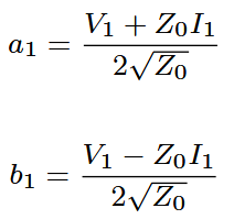
V and I are the complex voltage and current flowing into the port 1 with impedance Z0. It can be shown that |a1|2 and |b1|2 correspond to the power of the incedent wave and the power of the reflected wave. This derivation starts with the notion that power is transferred between a generator and the port using V, I and Z as parameters. Then a linear transformation is carried out using the above definition of a1 and b1. This transformation just gives us another projection to look at the power transfer. Not in terms of V and I but in a1 and b1. It can then be shown that a1 and b1 have a clear physical meaning, as the incident and reflected power. For those looking at the exact derivation, the article of K. Kurokawa is recommended (1965, "Power Waves and the Scattering Matrix").
As a1 and b1 stand for the traveling waves at the port, they correspond with the forward and backward traveling (reflected) waves V+ and V- along a transmission line. The only difference is that a1 and b1 are normalized at the square root of Z (1 / √Z). It is therefore not uncommon to find S-parameters calculated by using the traveling wave parameters V+ and V-.
2.2.1 Converting S-parameters to dB
We know that S-parameters can be calculated from the ratios of the traveling waves amplitudes V+ and V-. The square of these values correspond with the wave power |ax|2. So when we want to express an S-parameter value in dB, we have to use the formula 20Log(S).
Converting S-parameters to dB is often very convenient. It helps us to cope with a broad range of values. Which is the primary goal of the dB unit anyway. Some examples are (referring to figure 4):
Gain : 20Log (S21) dB
Input return loss : -20 Log (S11) dB
2.3 Other type of parameters
There also happen to be other types of parameters that can be used to describe a network. There are actually quite a few, all with their own specific applications. Here we mention the ABCD and T parameters. They are used for a property that S-parameters do not have: modeling a network of cascaded (sub)networks. ABCD and T parameter matrices can be multiplied to find the solution of the cascaded network. S parameters cannot do that. The transformation between two different parameter sets, for example from the S domain to the T domain (or vice versa), is mathematically simple.
So your network simulator will not work directly with S-parameters, but will first transfer them to a more suitable representation.
Another example of converting S parameters to T parameters (and vice versa) is the process of de-embedding S parameters to remove the effects of a test fixture.
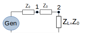
3. Relation between Return Loss and Impedance
It is important to realize that S11 is equivalent to the reflection coefficient Γ as defined in transmission theory. Both define the amount of reflected power. We also know that the amount of reflected energy at the end of a transmission line is defined by the impedance mismatch between Z0 and ZL (see figure 6). Therefore, if we know the reflection coefficient S11 and Z0, the impedance ZL can be calculated.
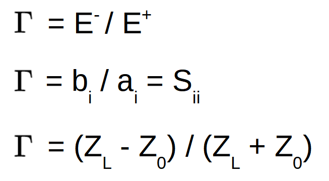
So, port impedance can be calculated by measuring the return loss and using the formula:
ZL = [ (1 + Γ) / (1 - Γ) ] . Z0
And, as Γ = S11:
ZL = [ (1 + S11) / (1 - S11) ] . Z0
There is a separate article about return loss measurements, since there is a lot more to say about this important subject.
4. S-parameter Matrices of Commonly Used RF circuits
It is instructive to study some examples of S-parameter matrices of commonly used RF structures. It gives you an idea of how to interpret an S-parameter matrix and often also increases your understanding of the RF device you are examining.
All examples assume ideal conditions. All ports are perfectly matched to Z0. We also ignore frequency-dependent behavior altogether.
In general, the S-parameters are calculated by using the definition for Sxy from section 2.1, and substituting ax and bx with the equations from section 2.2.
| RF Circuit | S-parameters | Description |
 |
 |
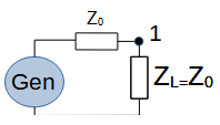
Perfect termination (1 port). It will reflect 0% of the incident wave. |
 |
 |
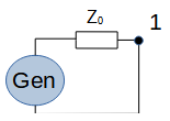
Short (1 port). It will reflect 100% of the incident wave and change its phase by 180 degrees. |
 |
 |
Open (1 port). It will reflect 100% of the incident wave. |
 |
 |
Isolator (2 port). Only waves traveling in a forward direction are allowed through. Waves that travel in the opposite direction are absorbed. An isolator is implemented using a circulator, which is actually a three port device. |
 |
 |
Series resistor Z0 (2 ports). The more general case is a resistor with the value 'Z'. In this case Sxx = Z / (2Z0+Z) and Sxy = (Z0+Z) / (2Z0+Z). |
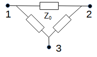 |
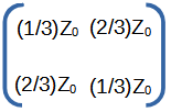
 |
6 dB Power splitter (3 ports). All three the resistors have an impedance of Z0. An alternative circuit uses a star arrangement of three resistors, each with an impedance of (1/3)*Z0. |
 |
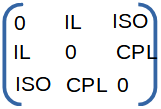 |
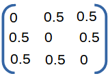
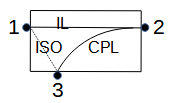
Coupler (3 port). With insertion loss (IL), coupling (CPL) and isolation (ISO). Directivity equals (ISO - IL - CPL). In a perfect coupler ISO would be 0. |
 |
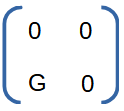 |
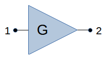
Amplifier (2 port) with gain G, perfect isolation and impedance match. |
 |
 |
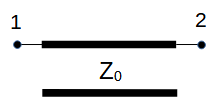
Transmission line (2 port) with line length L and β = 2π/λ. Lambda (λ) is the wave length in meter. |
 |
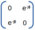 |
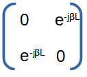
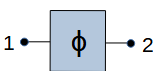
Phase shifter. Shifts phase by Φ with Φ in rad / s |
5. Measuring S-parameters
One of the advantages of using S-parameters is that they are relative easily measured due to the 50 Ohms reference impedance of the test ports. Compare this with the Y- and Z-parameter measurements. These are both difficult to measure and demanding for the D.U.T. Largely due to the test procedure which uses either open or shorted ports. The problem with open circuits and short circuits is that they are very difficult to create at high frequencies because of the ever-present parasitic capacitance and inductance. Maintaining a 50 ohm load at high frequencies is much easier to achieve. Hence the popularity of S-parameter measurements at RF and microwave frequencies.
The measurement of S-parameters is typically done with a Vector Network Analyzer (VNA) at the press of a button. Regular calibration of the measurement setup is an important step in this procedure, which often is taken care of by the VNA as well. The VNA will store the set S-parameters in a file that can be used as the device's S-parameters model. These files can be imported into network simulation software to analyze RF networks.
5.1 Measuring S-parameters of a Transistor
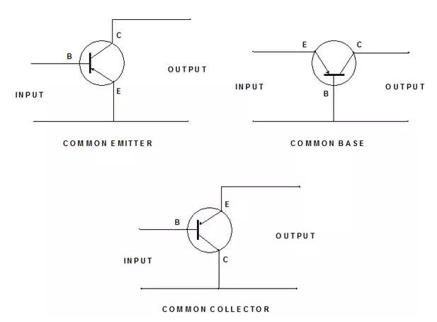
S-parameters are also used to model RF transistors. Although a transistor has three terminals, in all basic amplifier configuration there is always one terminal shared. Which leaves us with a two-port configuration. So don't expect three-port S-parameter models with transistors.
To measure a transistor with a VNA, it must be properly biased. This is achieved by using a Bias-T at each port of the VNA. Some sort of fixture is also needed to mount the transistor and make its terminals accessible through a standardized coaxial connector compatible with the VNA used. Some VNAs are equipped with an internal Bias-T to make it easier to measure devices that require a certain bias.
6. Using S-Parameters
As should be obvious by now, S-parameters are used to model all kinds of RF devices. These models are stored in S-parameter files by using the widely accepted Touchstone standard. Most RF simulators can import and use them to model the device in some RF network. There are a lot of on-line Touchstone viewers too.
The S-parameters themselves are mainly used in the field of measuring and defining RF devices. When used in a simulator, they are converted to a (matrix) representation that is more suitable for modeling the device and its effect in a larger network. It is worth noting that you cannot multiply S-parameter matrices to find the S-parameter matrix of a set of cascaded RF modules. This problem is usually solved by first converting the S parameters into T parameters. These types of parameters can be multiplied (in matrix format) to give you the response of a cascaded system. Then, this result can be back-transformed to find the matrix representation of the S-parameters of the cascaded RF modules. This approach also forms the basis of a technique for de-embedding the connectors of an RF measuring fixture.
6.1 Examples of S-parameter Plots
In practice, S-parameters are visualized as a graph to show the variation of the parameters over frequency. Usually the magnitude is shown in decibels so that both very large and small values can be easily displayed. These types of graphs are useful for understanding the performance of an RF module at a glance. You will find them in abundance in RF module datasheets.
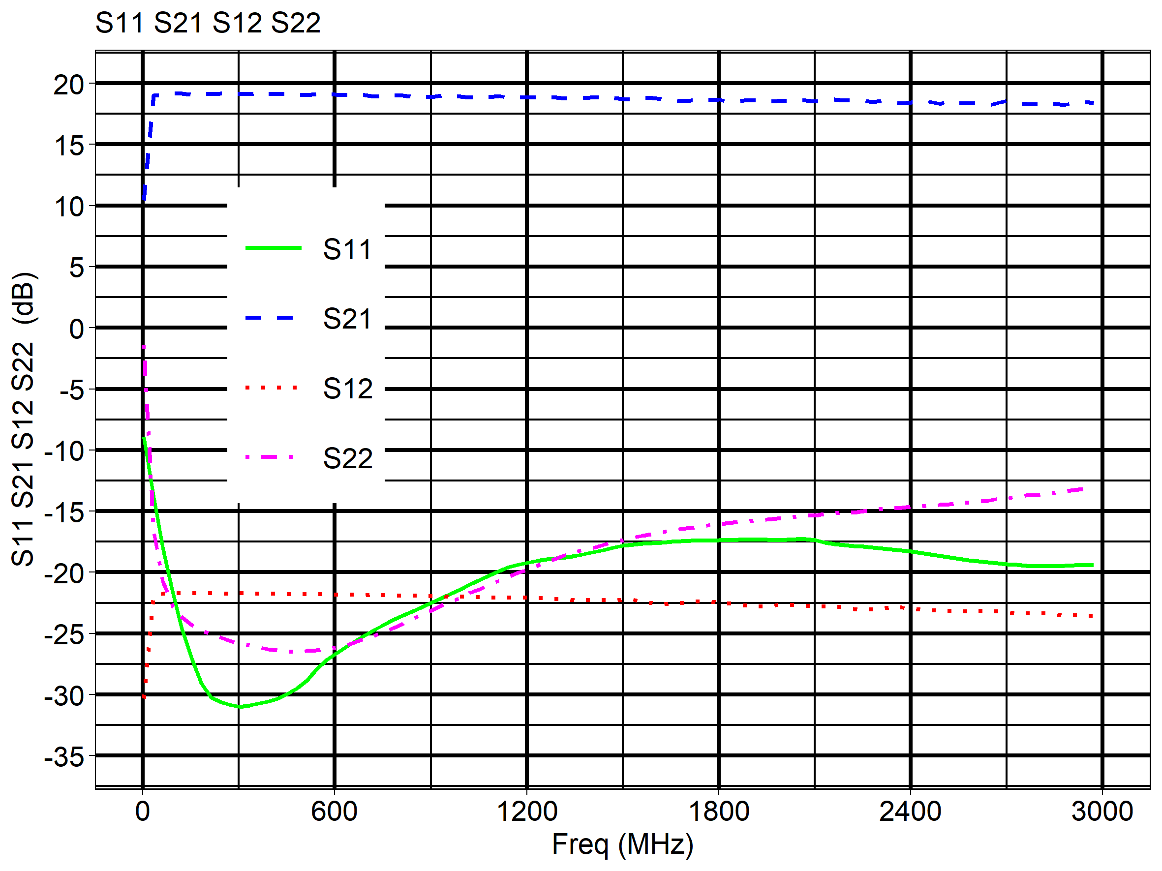
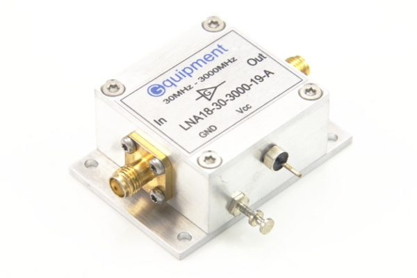
6.1.1 S-parameter Plot of an LNA
The first example is of the Low Noise Amplifier LNA18-30-3000-19-A. This is an LNA with a noise figure of only 1.8 dB and a flat gain of 19 dB over its entire frequency range from 30 MHz to 3 GHz. But of course it is easier to look at the S-parameter graph (Plot 1). In addition to gain (S21), the graph also shows the isolation (S12) and the quality of the port match against 50 ohms as S11 and s22 respectively.
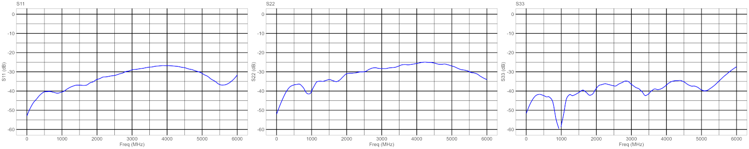
6.1.2 S-parameter Plot of an RF Splitter
Next is the RF module SPLT-3R1-0-6000-B which splits an RF signal in half (and vice versa). It is a broadband device that can be used from DC to 5 GHz. It is mainly used in test setups where one wants to split a signal or combine two signals. Plot 2 shows the insertion loss between all ports is 6 dB, which is typical for this type of module.
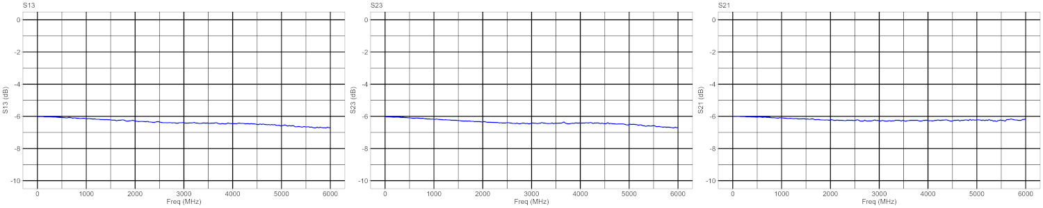
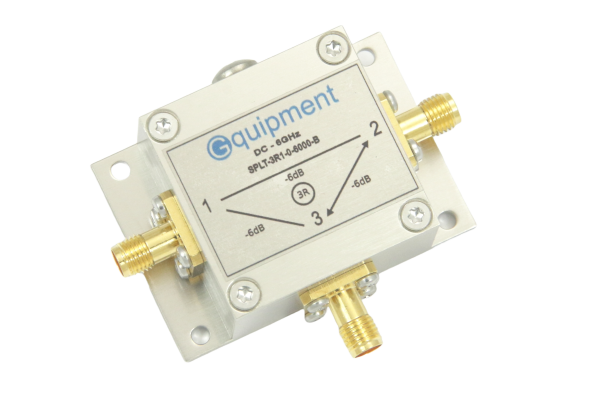
The plots also show that around DC, the S-parameters values almost are at their theoretical values. The insertion loss deviation stays within 1 dB over the full frequency range. A more important metric however is the balance (Bal) between the power at the output ports, which typically is much smaller then 1 dB.
Bal = S31/S32
Return loss tops around 3 GHz at approximate -20 dB, which is considered a good match.
7. Conclusion
S-parameters are an invaluable way to model RF devices. They are relatively easy to measure, can be used in RF circuit simulators and are a good way to evaluate RF devices because of the clear physical meaning of the S-parameters themselves.
It comes as no surprise that S-parameters are used extensively in the RF industry.